• Photonics Research
  • Vol. 11, Issue 8, 1474 (2023)
Yufei Liu1、2, Jialiang Sun1、2, Xinyu Li1、2, Shuxiao Wang1, Wencheng Yue1, Yan Cai1、*, and Mingbin Yu3
Author Affiliations
  • 1National Key Laboratory of Materials for Integrated Circuits, Shanghai Institute of Microsystem and Information Technology, Chinese Academy of Sciences, Shanghai 200050, China
  • 2University of Chinese Academy of Sciences, Beijing 100049, China
  • 3Shanghai Industrial μTechnology Research Institute, Shanghai 201800, China
  • show less
    DOI: 10.1364/PRJ.488474 Cite this Article Set citation alerts
    Yufei Liu, Jialiang Sun, Xinyu Li, Shuxiao Wang, Wencheng Yue, Yan Cai, Mingbin Yu. Thermally tunable GeSi electro-absorption modulator with a wide effective operating wavelength range[J]. Photonics Research, 2023, 11(8): 1474 Copy Citation Text show less
    (a) Schematic diagram of the thermal tuning structure. (b) Simulated temperature distribution when the heater power is 4.63 mW. (c)–(h) Simulated temperature distribution of waveguide when the heater power is (c) 1.37 mW, (d) 4.63 mW, (e) 6.47 mW, (f) 8.33 mW, (g) 10.1 mW, and (h) 11.73 mW.
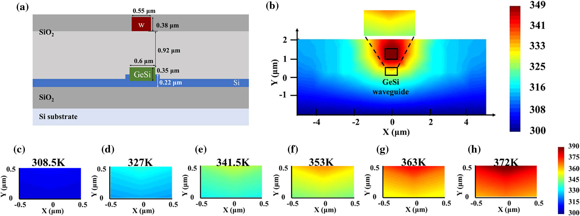
    Fig. 1. (a) Schematic diagram of the thermal tuning structure. (b) Simulated temperature distribution when the heater power is 4.63 mW. (c)–(h) Simulated temperature distribution of waveguide when the heater power is (c) 1.37 mW, (d) 4.63 mW, (e) 6.47 mW, (f) 8.33 mW, (g) 10.1 mW, and (h) 11.73 mW.
    (a) Absorption coefficient lines of Ge0.992Si0.008 at ON and OFF states. (b) FOM variation with wavelength at different temperatures.
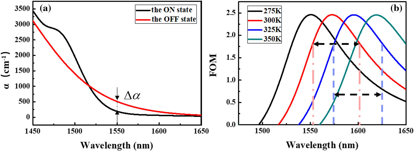
    Fig. 2. (a) Absorption coefficient lines of Ge0.992Si0.008 at ON and OFF states. (b) FOM variation with wavelength at different temperatures.
    Schematic diagram of (a) device structure, (b) cross section, and (c) SEM image.
    Fig. 3. Schematic diagram of (a) device structure, (b) cross section, and (c) SEM image.
    Electro-optical setup diagram. (a) DC link, (b) bandwidth link, and (c) eye diagram link.
    Fig. 4. Electro-optical setup diagram. (a) DC link, (b) bandwidth link, and (c) eye diagram link.
    Measured (a) transmission loss, (b) extinction ratios, and (c) fitting FOM of the EAM under different bias voltages.
    Fig. 5. Measured (a) transmission loss, (b) extinction ratios, and (c) fitting FOM of the EAM under different bias voltages.
    Measured (a) insertion loss and (b) extinction ratio at different heater power. (c) Fitting FOM at different heater power.
    Fig. 6. Measured (a) insertion loss and (b) extinction ratio at different heater power. (c) Fitting FOM at different heater power.
    (a) Measured transmission loss at 3 V reverse bias. (b) Wavelength changes with the heater power under 15 dB transmission loss at 3 V reverse bias.
    Fig. 7. (a) Measured transmission loss at 3 V reverse bias. (b) Wavelength changes with the heater power under 15 dB transmission loss at 3 V reverse bias.
    (a) Effect of light current and dark current as a function of DC bias. (b) 3 dB EO bandwidth of the device under different DC biases.
    Fig. 8. (a) Effect of light current and dark current as a function of DC bias. (b) 3 dB EO bandwidth of the device under different DC biases.
    80 Gbit/s NRZ eye diagrams of the EAM at different heater power: (a) 0 mW, (b) 1.37 mW, (c) 4.63 mW, (d) 6.47 mW, (e) 8.33 mW, and (f) 10.1 mW.
    Fig. 9. 80 Gbit/s NRZ eye diagrams of the EAM at different heater power: (a) 0 mW, (b) 1.37 mW, (c) 4.63 mW, (d) 6.47 mW, (e) 8.33 mW, and (f) 10.1 mW.
    (a) 80 Gbit/s NRZ electric eye diagram. (b)–(l) 80 Gbit/s NRZ eye diagrams of the EAM at different heater power: (b) 0 mW, (c) 0 mW, (d) 0 mW, (e) 1.37 mW, (f) 1.37 mW, (g) 4.63 mW, (h) 4.63 mW, (i) 6.47 mW, (j) 6.47 mW, (k) 8.33 mW, and (l) 10.1 mW.
    Fig. 10. (a) 80 Gbit/s NRZ electric eye diagram. (b)–(l) 80 Gbit/s NRZ eye diagrams of the EAM at different heater power: (b) 0 mW, (c) 0 mW, (d) 0 mW, (e) 1.37 mW, (f) 1.37 mW, (g) 4.63 mW, (h) 4.63 mW, (i) 6.47 mW, (j) 6.47 mW, (k) 8.33 mW, and (l) 10.1 mW.
    100 Gbit/s PAM4 eye diagrams of the EAM at different heater power: (a) 0 mW, (b) 1.37 mW, (c) 4.63 mW, (d) 6.47 mW, (e) 8.33 mW, and (f) 10.1 mW.
    Fig. 11. 100 Gbit/s PAM4 eye diagrams of the EAM at different heater power: (a) 0 mW, (b) 1.37 mW, (c) 4.63 mW, (d) 6.47 mW, (e) 8.33 mW, and (f) 10.1 mW.
    100 Gbit/s PAM4 eye diagrams of the EAM at different heater power: (a) 0 mW, (b) 0 mW, (c) 0 mW, (d) 1.37 mW, (e) 1.37 mW, (f) 4.63 mW, (g) 4.63 mW, (h) 6.47 mW, (i) 6.47 mW, (j) 8.33 mW, and (k) 10.1 mW.
    Fig. 12. 100 Gbit/s PAM4 eye diagrams of the EAM at different heater power: (a) 0 mW, (b) 0 mW, (c) 0 mW, (d) 1.37 mW, (e) 1.37 mW, (f) 4.63 mW, (g) 4.63 mW, (h) 6.47 mW, (i) 6.47 mW, (j) 8.33 mW, and (k) 10.1 mW.
    100 Gbit/s NRZ eye diagrams of the EAM at heater power (a) 0 mW and (b) 8.5 mW. 200 Gbit/s PAM4 eye diagrams of the EAM at heater power (c) 0 mW and (d) 8.5 mW.
    Fig. 13. 100 Gbit/s NRZ eye diagrams of the EAM at heater power (a) 0 mW and (b) 8.5 mW. 200 Gbit/s PAM4 eye diagrams of the EAM at heater power (c) 0 mW and (d) 8.5 mW.
    Yufei Liu, Jialiang Sun, Xinyu Li, Shuxiao Wang, Wencheng Yue, Yan Cai, Mingbin Yu. Thermally tunable GeSi electro-absorption modulator with a wide effective operating wavelength range[J]. Photonics Research, 2023, 11(8): 1474
    Download Citation