• Photonics Research
  • Vol. 11, Issue 8, 1474 (2023)
Yufei Liu1、2, Jialiang Sun1、2, Xinyu Li1、2, Shuxiao Wang1, Wencheng Yue1, Yan Cai1、*, and Mingbin Yu3
Author Affiliations
  • 1National Key Laboratory of Materials for Integrated Circuits, Shanghai Institute of Microsystem and Information Technology, Chinese Academy of Sciences, Shanghai 200050, China
  • 2University of Chinese Academy of Sciences, Beijing 100049, China
  • 3Shanghai Industrial μTechnology Research Institute, Shanghai 201800, China
  • show less
    DOI: 10.1364/PRJ.488474 Cite this Article Set citation alerts
    Yufei Liu, Jialiang Sun, Xinyu Li, Shuxiao Wang, Wencheng Yue, Yan Cai, Mingbin Yu. Thermally tunable GeSi electro-absorption modulator with a wide effective operating wavelength range[J]. Photonics Research, 2023, 11(8): 1474 Copy Citation Text show less

    Abstract

    We demonstrate a GeSi electro-absorption modulator with on-chip thermal tuning for the first time, to the best of our knowledge. Theoretical simulation proves that the device temperature can be tuned and the effective operating wavelength range can be broadened. When the heater power is 4.63 mW, the temperature of the waveguide increases by about 27 K and the theoretical operating wavelength range is broadened by 23.7 nm. The experimental results show that the optical transmission line shifted to the longer wavelength by 4.8 nm by every 1 mW heater power. The effective static operating wavelength range of the device is increased from 34.4 nm to 60.1 nm, which means it is broadened by 25.7 nm. The band edge shift coefficient of 0.76 nm/K is obtained by temperature simulation and linear fitting of the measured data. The device has a 3 dB EO bandwidth of 89 GHz at 3 V reverse bias, and the eye diagram measurement shows a data rate of 80 Gbit/s for non-return-to-zero on–off keying modulation and 100 Gbit/s for 4 pulse amplitude modulation in the 1526.8 nm to 1613.2 nm wavelength range as the heater power increases from 0 mW to 10.1 mW.

    1. INTRODUCTION

    As the mainstream technology of future data centers, high-speed optical interconnection will be widely used in infrastructure such as supercomputers, high-performance servers, and data centers, and will become the core component of new network communication systems [1,2]. Silicon photonics refers to the use of CMOS process platforms to integrate optoelectronic devices on silicon-on-insulator (SOI) wafers, including modulators [3,4], detectors [57], and various passive devices for functions such as transmission [8], multiplexing [9], polarization [10], and coupling [11].

    The high-speed optical modulator is the key element in silicon photonics. The modulator is required to achieve higher speed, smaller footprint, lower power consumption, and higher integration density in order to achieve the board-to-board, chip-to-chip, and even inter-chip optical connection. Most silicon-based optical modulators are based on the free carrier dispersion effect, mainly Mach–Zehnder interferometer (MZI) modulators and micro-ring modulators. However, manipulating the change of carrier concentration makes it difficult to achieve balance among speed, bandwidth, power consumption, and extinction ratio (ER). An ultrahigh-speed single silicon MZI modulator beyond 100 Gbit/s has been reported [12]. However, the MZI modulator suffers from a large footprint and high power consumption. The micro-ring modulator beyond 100 Gbaud has compact size and low power consumption, but the performance is easily affected by the process variation and operating temperature [13]. The GeSi electro-absorption modulator (EAM) utilizes the Franz–Keldysh (FK) effect of the GeSi material. At present, the best Ge/GeSi EAMs are generally less than 100 μm in length, and have bandwidths beyond 50 GHz and low power consumption [1416]. The Ge modulator reported by our team has a high rate of over 80 Gbit/s and an ultralow dynamic power consumption of only 6.348 fJ/bit [3]. 110 Gbit/s non-return-to-zero (NRZ) and 160 Gbit/s 4 pulse amplitude modulation (PAM4) ultrahigh-speed GeSi EAM has been reported [17]. In addition, GeSi EAM has been explored for O band applications, and a 60 Gbit/s high-speed modulator has been realized by using the quantum-confined Stark effect [18]. Therefore, the GeSi EAM has achieved good balance in size, performance, power consumption, speed, and process integration difficulty, and is very promising as a high-speed modulator for on-chip interconnection in the future.

    It has been reported that Ge and GeSi EAMs with an optical bandwidth of about 30 nm have been fabricated on a 220 nm SOI platform, and GeSi EAM with an optical bandwidth of about 40 nm has been fabricated on a 3 mm SOI platform [14,15,19]. GeSi EAMs can further broaden the effective operating wavelength range, enabling them to be better applied in the wavelength division multiplexing (WDM) field. On-chip thermal tuning to tune the wavelength of devices has been widely used in devices such as MZIs and ring modulators, phase shifters, filters, and grating couplers on Silicon Photonics (SiP) platforms [2027]. Considering the influence of temperature on the absorption properties of GeSi material, thermal tuning is achievable in the EAM. However, the previous research on thermal effects in EAMs mainly focused on adjusting the external temperature during testing, and theoretical analysis through simulation [16,2830]. In this paper, the on-chip thermally tunable GeSi EAM is realized for the first time, to the best of our knowledge, to broaden the effective operating wavelength range of the device and adjust the influence of process manufacturing and material composition deviations on the operating wavelength of the device. We added a tungsten (W) thermal tuning structure with a width of 0.55 μm and a height of 0.38 μm in a typical GeSi EAM device. It is proved by simulation that the temperature of the device can be adjusted through the thermal tuning to optimize the performance of the device and broaden the effective operating wavelength range of the EAM. During measurements, as the heat-tuned voltage increases, the heater power increases, and the insertion loss (IL) as well as the static extinction ratio curves shifts to longer wavelengths. When the heater power is 4.63 mW, the temperature of the waveguide increases by about 27 K through simulation. The measured effective static operating wavelength range of the device is increased from 34.4 nm to 60.1 nm, which is consistent with the simulation broadening results. When the heater power increases by 1 mW, the wavelength shifts 4.8 nm. A band edge shift coefficient of 0.76 nm/K is obtained by temperature simulation and linear fitting of the measured data. Limited by the rate of the measurement equipment, the device has clear 80 Gbit/s NRZ and 100 Gbit/s PAM4 eye diagrams in the 1526.8 nm to 1613.2 nm wavelength range as the thermal tuning power increases from 0 mW to 10.1 mW. In the measured effective operating wavelength range, the device has an NRZ rate exceeding 100 Gbit/s and a PAM4 rate exceeding 200 Gbit/s.

    2. MATERIAL ABSORPTION RESPONSE

    The GeSi EAM utilizes the FK effect of the GeSi material. When a bias voltage is applied to the GeSi material, the electric field strength will cause a change in the direct bandgap of the material, thereby changing the absorption coefficient of the material, so that the light can obtain modulation. Since the absorption of the direct bandgap is three orders of magnitude higher than the indirect one, the absorption of the indirect bandgap is negligible [31]. Under the assumption that the electric field applied in the material is a uniform electric field and the exciton effect between electrons and holes is ignored due to the effect of the external electric field, considering the influence of temperature on the semiconductor band, the absorption coefficient is modeled in Eq. (1), which comes from the Schrödinger equation of electron-hole pairs in the presence of an electric field with Fermi’s golden rule applied [32]: α(ω,T)=e2Ep(T)12nrcε0m0ω×{(2mr,lh2)32θF,lh{ηlh(T)Ai2[ηlh(T)]+Ai2[ηlh(T)]}+(2mr,hh2)32θF,hh{ηhh(T)Ai2[ηhh(T)]+Ai2[ηhh(T)]}},where ω is the angular frequency, e is the elementary charge, Ep is the matrix constant related to the material, nr is the refractive index of the material, c is the speed of light in vacuum, ε0 is the dielectric constant in vacuum, m0 is the mass of free electrons, is the parsimonious Planck constant, mr,lh=meΓmlh/(meΓ+mlh) is the parsimonious effective mass of light holes in the Γ valley, θF,lh=[2e2F2/(2mr,lh)]1/3, F is the electric field strength, ηlh(T)=[Egd(T)+ΔEglh(T)ω]/θF,lh, and the parameters of the formula of mr,hh, θF,hh, and ηhh(T) related to heavy holes are completely analogous to those of light holes. For the GeSi composite material, when the silicon component is less than 2%, the linear difference method can be used to obtain the material bandgap [Eg(Ge1xSix)=(1x)Eg(Ge)+xEg(Si)]. Among them, the direct bandgap of Si is 4.06 eV, and that of Ge is 0.80 eV. The influence of temperature on the material bandgap can be expressed as [33] Eg(T)=E0αT2/(T+β), where Eg(T) represents the forbidden bandwidth affected by temperature, E0 is the forbidden bandwidth at zero Kelvin (K), T is the Kelvin temperature, and α and β are constant factors.

    3. DESIGN OF THERMAL TUNING AND DEVICE

    The choice of materials for the overhead heater is limited to CMOS compatible materials in the process flow. The resistivity and melting point of W are 8 μΩ cm and 3417°C, respectively, higher than those of Cu (1.68 μΩ cm and 1083°C) used as the metal electrode, which means that the W heater has a low drive current and can operate at higher temperatures [24]. Also, the higher resistivity of W can ensure that most heat dissipation of the current is in the W heater. We design the heater structure (width=0.55  μm and height=0.38  μm) of the GeSi EAM according to the actual processing, which is on the SOI platform with the distance of 0.92 μm from the rib waveguide, as shown in Fig. 1(a). The GeSi waveguide has a width of 0.6 μm and a height of 0.35 μm. We simulate the temperature distribution of the on-chip thermal tuning with a heating power of 4.63 mW with Lumerical’s 3D Heat Transport Simulator in Fig. 1(b). When the heater power is 4.63 mW, the temperature of the heat source is 349 K, while the temperature of the center of the waveguide is about 327 K. As shown in Figs. 1(c)–1(g), by continuously pressurizing the thermal tuning structure and increasing the heater power from 1.37 mW to 11.73 mW, it can be seen that as the temperature of the heat source increases, the temperature of the GeSi waveguide also gradually increases.

    (a) Schematic diagram of the thermal tuning structure. (b) Simulated temperature distribution when the heater power is 4.63 mW. (c)–(h) Simulated temperature distribution of waveguide when the heater power is (c) 1.37 mW, (d) 4.63 mW, (e) 6.47 mW, (f) 8.33 mW, (g) 10.1 mW, and (h) 11.73 mW.

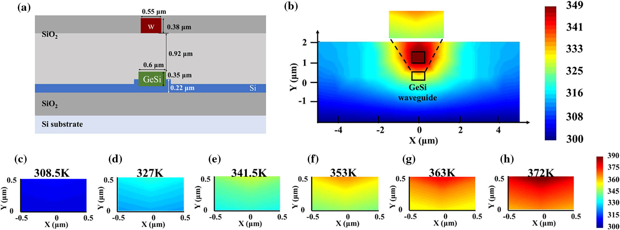
    Figure 1.(a) Schematic diagram of the thermal tuning structure. (b) Simulated temperature distribution when the heater power is 4.63 mW. (c)–(h) Simulated temperature distribution of waveguide when the heater power is (c) 1.37 mW, (d) 4.63 mW, (e) 6.47 mW, (f) 8.33 mW, (g) 10.1 mW, and (h) 11.73 mW.

    According to the calculation method of the absorption coefficient based on the FK effect mechanism in Eq. (1), we simply simulated the performance of the device under ideal conditions. Usually, the post-growth annealing temperature used for the epitaxially grown GeSi material is 850°C, and the in-plane stress introduced by it is about 0.2% [32]. We chose the Ge0.992Si0.008 compound semiconductor with a fixed ratio of silicon composition, and calculated the absorption lines of the semiconductor at room temperature (T=300  K), as shown in the curve in Fig. 2(a). The difference in the absorption coefficient (Δα=αoffαon) between the OFF state (when a 3 V reverse bias is applied, the electric field applied to the GeSi material is about 74 kV/cm) and the ON state (the built-in electric field strength is about 12 kV/cm) of the material is large at around 1550 nm. For EA modulators, we usually use the form of FOM=ER/IL=Δα/αon to evaluate the performance of the device, where ER=10lg(eαoffLeαonL)=4.343(αoffαon) and IL=10lg(eαonL)=4.343αonL. In addition, we also calculated the variation of FOM at 3 V reverse bias with wavelength at different temperatures, as shown in Fig. 2(b). It can be clearly seen that when the temperature changes from 275 K to 325 K, the corresponding wavelength of the FOM peak is red shifted from 1550 nm to 1600 nm, and when the temperature is lowered, there will be a blue shift to a shorter wavelength. Therefore, we believe that the operating wavelength range of the device can be effectively broadened by adjusting the operating wavelength of the device through on-chip thermal adjustment. It can be seen that the effective operating wavelength range (which we define as the wavelength range that the FOM decreases from the peak value to 0.707 times the peak value [28]) of the device increases from 53.1 nm to 76.8 nm when the temperature is increased by 25 K, and the operating wavelength range is broadened by 23.7 nm.

    (a) Absorption coefficient lines of Ge0.992Si0.008 at ON and OFF states. (b) FOM variation with wavelength at different temperatures.

    Figure 2.(a) Absorption coefficient lines of Ge0.992Si0.008 at ON and OFF states. (b) FOM variation with wavelength at different temperatures.

    4. FABRICATION AND MEASUREMENT RESULTS

    Figure 3 shows a schematic structure of the EAM device, which is fabricated in imec’s silicon photonics platform on SOI wafers with a 220 nm top Si thickness. The GeSi material is selectively grown in a recessed Si region using reduced pressure chemical vapor deposition as in Ref. [14]. As shown in the SEM image of the device in Fig. 3(c), the basic structure of the device is the same as the simulated cross-sectional schematic, in which the width of the intrinsic region without P/N implantation is 450 nm, and the P and N doping concentrations of Ge regions are about 7×10¹⁶  cm3. The fabricated device has a length of 40 μm.

    Schematic diagram of (a) device structure, (b) cross section, and (c) SEM image.

    Figure 3.Schematic diagram of (a) device structure, (b) cross section, and (c) SEM image.

    The performance of the EAM is first measured using the setup illustrated in Fig. 4(a) with the Keysight 8164B lightwave measurement system (81606A tunable laser source and 81635A optical power sensor), Thorlabs EPC561 fiber polarization controller, DC probe, and Keysight 2450 source meter. Figure 5(a) shows the transmission loss of the device from 0 V to 3 V reverse bias voltage at room temperature, which is calculated by subtracting the coupling loss. The coupling loss is derived for the reference structure without EAM, since the optical loss of the reference structure contained the coupling loss of the same two grating couplers. Besides, the resulting transmission loss at 0 V reverse bias is the insertion loss of the device. The extinction ratio from 1 V to 3 V reverse bias is obtained, as shown in Fig. 5(b). To assess the EAM performance, we use a figure of merit (FOM=ER/IL). As shown in Fig. 5(c), the maximum fitting FOM of the EAM is 1.35 at the wavelength of 1543.6 nm at 3 V reverse bias voltage. At the wavelength of 1543.6 nm, the insertion loss of the EAM is about 3.89 dB, while the extinction ratio of the device is about 5.24 dB.

    Electro-optical setup diagram. (a) DC link, (b) bandwidth link, and (c) eye diagram link.

    Figure 4.Electro-optical setup diagram. (a) DC link, (b) bandwidth link, and (c) eye diagram link.

    Measured (a) transmission loss, (b) extinction ratios, and (c) fitting FOM of the EAM under different bias voltages.

    Figure 5.Measured (a) transmission loss, (b) extinction ratios, and (c) fitting FOM of the EAM under different bias voltages.

    Subsequently, we applied voltages to the thermal tuning structure; as shown in Fig. 6, as the heat-tuned voltage increases, the heater power increases, and the spectral line moves to the long-wavelength direction. This also demonstrates for the first time, to the best of our knowledge, the feasibility of using the on-chip thermal tuning in the GeSi EAMs. The heater power is obtained by the formula P=I2R, where the current is obtained by applying a bias voltage to the heater structure, and the resistance of the heater structure is calculated according to the size of the heater structure and the resistivity of tungsten. In Figs. 6(a) and 6(b), we show the measured insertion loss and extinction ratio for five thermally tuned power settings. The extinction ratio decreases with increasing temperature, which is inconsistent with reliability measurements from Ref. [33]. It is possible that due to the pre-existing defects on the Ge/Si and Ge/Ox interfaces, when a reverse bias voltage is applied, the loss of the device will increase with the increase of temperature, and the ER will change with temperature. Further optimization of the process is required to reduce defects and increase the yield of the devices at wafer level. Figure 6(c) shows the FOM of the device at different heater powers. At room temperature, the effective operating wavelength range of the device is from 1526.8 nm to 1561.2 nm, while when the heater power is 4.63 mW, the effective operating wavelength range of the device is from 1545.2 nm to 1586.9 nm. In the processing of increasing the thermal regulation efficiency from 0 to 4.63 mW, the temperature of the waveguide is increased by about 27 K through simulation, the effective operating wavelength range of the device is widened from 34.4 nm to 60.1 nm, and the wavelength is broadened by 25.7 nm, which is consistent with the broadening results simulated in Fig. 2(b). In the range of heater power from 0 mW to 10.1 mW, the transmission loss of the device at 3 V reverse bias is shown in Fig. 7(a). According to the wavelength variation under 15 dB transmission loss, the performances of the device are fitted, and when the heater power increases by 1 mW, the optical transmission line will shift by 4.8 nm as shown in Fig. 7(b). The band edge shift coefficient of 0.76 nm/K is obtained by temperature simulation and linear fitting of the measured data, which is comparable with the theoretical value [28].

    Measured (a) insertion loss and (b) extinction ratio at different heater power. (c) Fitting FOM at different heater power.

    Figure 6.Measured (a) insertion loss and (b) extinction ratio at different heater power. (c) Fitting FOM at different heater power.

    (a) Measured transmission loss at 3 V reverse bias. (b) Wavelength changes with the heater power under 15 dB transmission loss at 3 V reverse bias.

    Figure 7.(a) Measured transmission loss at 3 V reverse bias. (b) Wavelength changes with the heater power under 15 dB transmission loss at 3 V reverse bias.

    The 3 dB bandwidths were tested on the high frequency platform at the National Information Optoelectronics Innovation Center. As shown in Fig. 8(a), at 3 V reverse bias, the dark current of the EAM is 220 nA, and the static power consumption of the device can be estimated as mean current multiplied by DC bias voltage, which is 1.65 mW at 3 V reverse voltage when the input light intensity is 3.16 mW at room temperature. It can be seen from Fig. 8(b) that the 3 dB EO bandwidth of the device exceeds 80 GHz under 1 V reverse bias, and the EO bandwidth of the device reaches 89 GHz at 3 V reverse bias at room temperature. According to the RC parameters extracted from the S parameter curve, the extracted junction capacitance of the EAM is estimated to be 3.7 fF, with the series resistance of 240 Ω, which indicates an RC-limited bandwidth beyond 150 GHz. Affected by the design of the GS electrode, the test calibration and practical application frequency range of the GS electrode will be limited when the frequency exceeds 80 GHz, resulting in a significant drop in the S parameters of the results after exceeding 80 GHz.

    (a) Effect of light current and dark current as a function of DC bias. (b) 3 dB EO bandwidth of the device under different DC biases.

    Figure 8.(a) Effect of light current and dark current as a function of DC bias. (b) 3 dB EO bandwidth of the device under different DC biases.

    Eye diagrams are measured to explore the high-speed performance of the EAM, as shown in Fig. 4(c). 80 Gbit/s (2111) NRZ pseudorandom binary sequence (PRBS) electrical signals are generated by a bit pattern generator. These electrical signals are amplified by RF amplifiers to a peak-to-peak voltage (Vpp) of 1.5 V. Due to the rate limitation of the measurement equipment (whose theoretical maximum rate is 60 Gbaud), at the rate of 80 Gbit/s the electrical eye diagram results shown in Fig. 10(a) will have nonlinear phenomena. Figures 9(a)–9(f) show the eye diagram results of the device at the optimal operating wavelength under different heater powers at 3 V reverse bias. Figures 10(b)–10(l) show the eye diagram results in the extreme effective operating wavelength range and at the wavelength of 1555 nm. The eye diagram results are stable with the increase of heater power at the wavelength of 1555 nm. When the heater power exceeds 6.47 mW, due to the lateral shift of the optical transmission line, the output optical power of the device is low, which is limited by the detection of the measurement equipment and cannot be measured. At room temperature, the device has a clear eye diagram in the wavelength range of 1526.8 nm to 1561.2 nm, and the dynamic effective operating wavelength range of the device is consistent with the static state. When the thermal regulation is applied to 4.63 mW, the EAM still has a clear eye diagram at a wavelength of 1586.9 nm, which shows that the dynamic effective operating wavelength range of the device is increased to 60.1 nm by introducing on-chip thermal tuning. When the thermal tuning is applied to 10.1 mW, the clear eye diagram is at 1613.2 nm. The dynamic power consumption per bit could be estimated by (CjVpp2)/4 [34]. The Cj and the Vpp of the EAM are 3.7 fF and 1.5Vpp. Thus, the dynamic power consumption of the device is 2.08 fJ/bit. Figures 11(a)–11(f) also show the 100 Gbit/s PAM4 eye diagram results of the EAM at the optimal operating wavelength under different heater powers at 3 V reverse bias, and Figs. 12(a)–12(k) show the eye diagram results in the extreme effective operating wavelength range and at the wavelength of 1555 nm. These electrical signals are amplified by RF amplifiers to a peak-to-peak voltage (Vpp) of 2.7 V. When the thermal regulation is applied to 10.1 mW, the device still has a clear 100 Gbit/s PAM4 eye diagram at a wavelength of 1613.2 nm, whose dynamic extinction ratio is 5.657 dB. Figures 13(a)–13(d) show the test results of the National Information Optoelectronics Innovation Center. When the thermal regulation is applied to 8.5 mW, the device still has clear 100 Gbit/s NRZ and 200 Gbit/s PAM4 eye diagrams at a wavelength of 1602 nm, whose dynamic extinction ratios are 2.299 dB and 2.19 dB, which means that the device has an NRZ modulation rate of over 100 Gbit/s. On-chip thermal tuning can well broaden the effective operating wavelength range of the device while maintaining the high-speed and excellent performance of the device. Due to the compatibility of the process, the performance of the device is improved without increasing the difficulty of process manufacturing. This provides new broadband high-performance EAMs for high-density optoelectronic integration and optical transceiver modules.

    80 Gbit/s NRZ eye diagrams of the EAM at different heater power: (a) 0 mW, (b) 1.37 mW, (c) 4.63 mW, (d) 6.47 mW, (e) 8.33 mW, and (f) 10.1 mW.

    Figure 9.80 Gbit/s NRZ eye diagrams of the EAM at different heater power: (a) 0 mW, (b) 1.37 mW, (c) 4.63 mW, (d) 6.47 mW, (e) 8.33 mW, and (f) 10.1 mW.

    (a) 80 Gbit/s NRZ electric eye diagram. (b)–(l) 80 Gbit/s NRZ eye diagrams of the EAM at different heater power: (b) 0 mW, (c) 0 mW, (d) 0 mW, (e) 1.37 mW, (f) 1.37 mW, (g) 4.63 mW, (h) 4.63 mW, (i) 6.47 mW, (j) 6.47 mW, (k) 8.33 mW, and (l) 10.1 mW.

    Figure 10.(a) 80 Gbit/s NRZ electric eye diagram. (b)–(l) 80 Gbit/s NRZ eye diagrams of the EAM at different heater power: (b) 0 mW, (c) 0 mW, (d) 0 mW, (e) 1.37 mW, (f) 1.37 mW, (g) 4.63 mW, (h) 4.63 mW, (i) 6.47 mW, (j) 6.47 mW, (k) 8.33 mW, and (l) 10.1 mW.

    100 Gbit/s PAM4 eye diagrams of the EAM at different heater power: (a) 0 mW, (b) 1.37 mW, (c) 4.63 mW, (d) 6.47 mW, (e) 8.33 mW, and (f) 10.1 mW.

    Figure 11.100 Gbit/s PAM4 eye diagrams of the EAM at different heater power: (a) 0 mW, (b) 1.37 mW, (c) 4.63 mW, (d) 6.47 mW, (e) 8.33 mW, and (f) 10.1 mW.

    100 Gbit/s PAM4 eye diagrams of the EAM at different heater power: (a) 0 mW, (b) 0 mW, (c) 0 mW, (d) 1.37 mW, (e) 1.37 mW, (f) 4.63 mW, (g) 4.63 mW, (h) 6.47 mW, (i) 6.47 mW, (j) 8.33 mW, and (k) 10.1 mW.

    Figure 12.100 Gbit/s PAM4 eye diagrams of the EAM at different heater power: (a) 0 mW, (b) 0 mW, (c) 0 mW, (d) 1.37 mW, (e) 1.37 mW, (f) 4.63 mW, (g) 4.63 mW, (h) 6.47 mW, (i) 6.47 mW, (j) 8.33 mW, and (k) 10.1 mW.

    100 Gbit/s NRZ eye diagrams of the EAM at heater power (a) 0 mW and (b) 8.5 mW. 200 Gbit/s PAM4 eye diagrams of the EAM at heater power (c) 0 mW and (d) 8.5 mW.

    Figure 13.100 Gbit/s NRZ eye diagrams of the EAM at heater power (a) 0 mW and (b) 8.5 mW. 200 Gbit/s PAM4 eye diagrams of the EAM at heater power (c) 0 mW and (d) 8.5 mW.

    5. CONCLUSION

    A horizontal GeSi waveguide EAM with an on-chip thermal tuning structure is demonstrated for the first time, to the best of our knowledge. First, it is proved by simulation that the temperature of the device can be adjusted through the thermal tuning to optimize the performance of the device and broaden the effective operating wavelength range of the EAM. Afterwards, GeSi EAM devices are fabricated, and their performance is measured. The device has an insertion loss of 3.89 dB at a wavelength of 1543.6 nm at room temperature and a static extinction ratio of 5.236 dB at 3 V reverse bias. As the heat-tuned voltage increases, the heater power increases, and the insertion loss, static extinction ratio, and FOM curves shift to longer wavelengths. When the heater power is 4.63 mW, the effective static operating wavelength range of the device is increased from 34.4 nm to 60.1 nm, and the wavelength is broadened by 25.7 nm. According to the wavelength change at 15 dB transmission loss, when the heater power increases by 1 mW, the optical transmission line shifts 4.8 nm. The band edge shift coefficient of 0.76 nm/K is obtained by temperature simulation and linear fitting of the measured data. The EAM has a 3 dB EO bandwidth of 89 GHz at 3 V reverse bias, and the device has clear 100 Gbit/s NRZ and 200 Gbit/s PAM4 eye diagrams in a large effective operating wavelength range. When the thermal regulation efficiency is 4.63 mW, the dynamic effective operating wavelength range of the device is from 1526.8 nm to 1586.9 nm, which is consistent with the static performance of the device. The dynamic power consumption of the device is 2.08 fJ/bit, and the total dynamic power consumption is 45.2 fJ/bit including the thermal tuning power consumption with a heater power of 4.63 mW. Although this power consumption value is still lower than that of the MZI modulators, the introduction of thermal control does increase the power consumption of the device. In the future, the undercut structure of the silicon substrate under the thermal tuning structure can be adopted to further reduce the thermal power consumption, which is realized by preventing the heat from leaking out of the device due to the presence of the air isolation layer. The EAM with on-chip thermal tuning has a large effective operating wavelength range and ultrahigh-speed performance, and is fully compatible with conventional silicon photonics process flows, which provides new broadband and high-performance EAMs for high-density optoelectronic integration and optical transceiver modules.

    References

    [1] C. Kachris, I. Tomkos. A survey on optical interconnects for data centers. Commun. Surveys Tuts., 14, 1021-1036(2012).

    [2] Y. Liu, S. Wang, J. Wang, X. Li, M. Yu, Y. Cai. Silicon photonic transceivers in the field of optical communication. Nano Commun. Netw., 31, 100379(2022).

    [3] Y. Liu, J. Sun, R. Song, X. Li, J. Wang, S. Wang, Y. Yu, W. Yue, Y. Cai, M. Yu. 80 Gb/s NRZ Ge waveguide electro-absorption modulator. Opt. Express, 30, 34276-34286(2022).

    [4] J. Zhou, J. Wang, L. Zhu, Q. Zhang. Silicon photonics for 100 Gbaud. J. Lightwave Technol., 39, 857-867(2020).

    [5] X. Li, Y. Liu, R. Song, C. Li, S. Wang, W. Yue, Z. Tu, X. Chen, Y. Cai, W. Wang, M. Yu. PIC-integrable high-responsivity germanium waveguide photodetector in the C+L band. Opt. Express, 31, 3325-3335(2023).

    [6] X. Li, J. Wang, Y. Liu, J. Chen, Y. Du, W. Wang, Y. Cai, J. Ma, M. Yu. Design of Ge1-xSnx-on-Si waveguide photodetectors featuring high-speed high-sensitivity photodetection in the C- to U-bands. Appl. Opt., 59, 7646-7651(2020).

    [7] M. Romagnoli, S. Marconi, M. A. Giambra, A. Montanaro, V. Mišeikis, S. Soresi, S. Tirelli, P. Galli, F. Buchali, W. Templ, C. Coletti, V. Sorianello. High-data-rate photothermal effect graphene detector integrated in a SOI waveguide. Proc. SPIE, 11711, 1171106(2021).

    [8] W. Shi, Y. Tian, A. Gervais. Scaling capacity of fiber-optic transmission systems via silicon photonics. Nanophotonics, 9, 4629-4663(2020).

    [9] R. B. Priti, O. Liboiron-Ladouceur. A reconfigurable multimode demultiplexer/switch for mode-multiplexed silicon photonics interconnects. IEEE J. Sel. Top. Quantum Electron., 24, 8300810(2018).

    [10] W. D. Sacher, T. Barwicz, B. J. F. Taylor, J. K. S. Poon. Polarization rotator-splitters in standard active silicon photonics platforms. Opt. Express, 22, 3777-3786(2014).

    [11] A. Bozzola, L. Carroll, D. Gerace, I. Cristiani, L. C. Andreani. Optimising apodized grating couplers in a pure SOI platform to −0.5 dB coupling efficiency. Opt. Express, 23, 16289-16304(2015).

    [12] G. T. Reed, S. Liu, D. J. Thomson, W. Zhang, F. Meng, X. Yan, C. G. Littlejohns, H. Du, W. Cao, M. Banakar, M. Ebert, V. Jeyaselvan, D. Tran, P. Petropoulos, L. Ke. Beyond 100 Gb/s from a single silicon MZI modulator. CLEO: Science and Innovations, SM5G-1(2022).

    [13] M. Sakib. Micro-ring modulators for next generation energy-efficient optical networks beyond 100 Gbaud. Proc. SPIE, PC12007, PC1200706(2022).

    [14] S. A. Srinivasan, P. Verheyen, R. Loo, I. D. Wolf, M. Pantouvaki, G. Lepage, S. Balakrishnan, W. Vanherle, P. Absil, J. V. Campenhout. 50 Gb/s C-band GeSi waveguide electro-absorption modulator. Optical Fiber Communication Conference, Tu3D.7(2016).

    [15] Z. Liu, X. Li, C. Niu, J. Zheng, C. Xue, Y. Zuo, B. Cheng. 56 Gbps high-speed Ge electro-absorption modulator. Photon. Res., 8, 1648-1652(2020).

    [16] D. Feng, S. Liao, H. Liang, J. Fong, B. Bijlani, R. Shafiiha, B. J. Luff, Y. Luo, J. Cunningham, A. V. Krishnamoorthy, M. Asghari. High speed GeSi electro-absorption modulator at 1550 nm wavelength on SOI waveguide. Opt. Express, 20, 22224-22232(2012).

    [17] H. Xiao, D. Wu, Y. Zhang, H. Zhang, D. Chen, M. Liu, J. Liu, L. Wang, X. Xiao, S. Yu. 110 Gbit/s NRZ and 160 Gbit/s PAM-4 GeSi electro-absorption modulator. Optical Fiber Communications Conference and Exhibition (OFC), 1-3(2022).

    [18] S. A. Srinivasan, C. Porret, S. Balakrishnan, Y. Ban, R. Loo, P. Verheyen, J. Van Campenhout, M. Pantouvaki. 60 Gb/s waveguide-coupled O-band GeSi quantum-confined Stark effect electro-absorption modulator. Optical Fiber Communication Conference, Tu1D-3(2021).

    [19] D. Feng, W. Qian, H. Liang, C. Kung, Z. Zhou, Z. Li, J. S. Levy, R. Shafiiha, J. Fong, B. J. Luff, M. Asghari. High-speed GeSi electroabsorption modulator on the SOI waveguide platform. IEEE J. Sel. Top. Quantum Electron., 19, 64-73(2013).

    [20] J. Sun, R. Kumar, M. Sakib, J. B. Driscoll, H. Jayatilleka, H. Rong. A 128 Gb/s PAM4 silicon microring modulator with integrated thermo-optic resonance tuning. J. Lightwave Technol., 37, 110-115(2018).

    [21] G. Li, X. Zheng, J. Yao, H. Thacker, I. Shubin, Y. Luo, K. Raj, J. E. Cunningham, A. V. Krishnamoorthy. 25 Gb/s 1V-driving CMOS ring modulator with integrated thermal tuning. Opt. Express, 19, 20435-20443(2011).

    [22] A. Ribeiro, S. Dwivedi, W. Bogaerts. A thermally tunable but athermal silicon MZI filter. 18th European Conference on Integrated Optics (ECIO), o-25(2016).

    [23] G. Li, X. Zheng, H. Thacker, J. Yao, Y. Luo, I. Shubin, K. Raj, J. E. Cunningham, A. V. Krishnamoorthy. 40 Gb/s thermally tunable CMOS ring modulator. The 9th International Conference on Group IV Photonics (GFP), 1-3(2012).

    [24] A. Masood, M. Pantouvaki, D. Goossens, G. Lepage, P. Verheyen, J. V. Campenhout, P. Absil, D. Van Thourhout, W. Bogaerts. Fabrication and characterization of CMOS-compatible integrated tungsten heaters for thermo-optic tuning in silicon photonics devices. Opt. Mater. Express, 4, 1383-1388(2014).

    [25] A. Masood, M. Pantouvaki, D. Goossens, G. Lepage, P. Verheyen, D. Van Thourhout, P. Absil, W. Bogaerts. CMOS-compatible tungsten heaters for silicon photonic waveguides. The 9th International Conference on Group IV Photonics (GFP), 234-236(2012).

    [26] Q. Fang, J. Song, X. Luo, L. Jia, M. Yu, G. Lo, Y. Liu. High efficiency ring-resonator filter with NiSi heater. IEEE Photon. Technol. Lett., 24, 350-352(2011).

    [27] S. Gao, H. Lin, L. Zhou, L. Liu, M. He, J. Xu, L. Chen, Y. Luo, X. Cai. Power-efficient thermal optical tunable grating coupler based on silicon photonic platform. IEEE Photon. Technol. Lett., 31, 537-540(2019).

    [28] L. Wu, Y. Zhou, Y. Cai, X. Cao, R. Wang, M. Qi, J. Fong, D. Feng, A. Wu. Design of a broadband Ge1−xSix electro-absorption modulator based on the Franz-Keldysh effect with thermal tuning. Opt. Express, 28, 7585-7595(2020).

    [29] J. Fujikata, M. Noguchi, R. Katamawari, K. Inaba, H. Ono, D. Shimura, Y. Onawa, H. Yaegashi, Y. Ishikawa. High-performance Ge/Si electro-absorption optical modulator up to 85°C and its highly efficient photodetector operation. Opt. Express, 31, 10732-10743(2023).

    [30] A. Tsiara, S. A. Srinivasan, S. Balakrishnan, M. Pantouvaki, P. Absil, J. Van Campenhout, K. Croes. Electrical and optical reliability analysis of GeSi electro-absorption modulators. Optical Fiber Communication Conference, M2A.5(2020).

    [31] A. Frova, P. Handler. Franz-Keldysh effect in the space-charge region of a germanium p−n junction. Phys. Rev., 137, A1857-A1861(1965).

    [32] J. Liu. GeSi Photodetectors and Electro-Absorption Modulators for Si Electronic-Photonic Integrated Circuits(2007).

    [33] Y. P. Varshni. Temperature dependence of the energy gap in semiconductors. Physica, 34, 149-154(1967).

    [34] S. A. Srinivasan, M. Pantouvaki, S. Gupta, H. T. Chen, P. Verheyen, G. Lepage, G. Roelkens, K. Saraswat, D. Van Thourhout, P. Absil, J. V. Campenhout. 56 Gb/s germanium waveguide electro-absorption modulator. J. Lightwave Technol., 34, 419-424(2016).

    Yufei Liu, Jialiang Sun, Xinyu Li, Shuxiao Wang, Wencheng Yue, Yan Cai, Mingbin Yu. Thermally tunable GeSi electro-absorption modulator with a wide effective operating wavelength range[J]. Photonics Research, 2023, 11(8): 1474
    Download Citation