• Opto-Electronic Advances
  • Vol. 5, Issue 1, 200046 (2022)
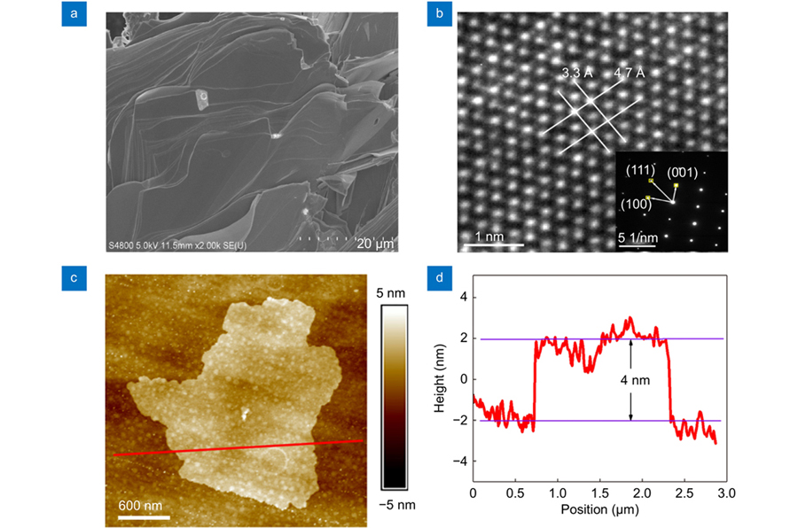
Leiming Wu1、2、4、†, Taojian Fan1、†, Songrui Wei1、†, Yijun Xu1, Ye Zhang1, Dingtao Ma1、2, Yiqing Shu2, Yuanjiang Xiang1, Jun Liu1, Jianqing Li2, Krassimir Panajotov3, Yuwen Qin4, and Han Zhang1、*
Author Affiliations
  • 1Institute of Microscale Optoelectronics, Collaborative Innovation Centre for Optoelectronic Science & Technology, Key Laboratory of Optoelectronic Devices and Systems of Ministry of Education and Guangdong Province, Shenzhen Key Laboratory of Micro-Nano Photonic Information Technology, Guangdong Laboratory of Artificial Intelligence and Digital Economy (SZ), Shenzhen University, Shenzhen 518060, China
  • 2Faculty of Information Technology, Macau University of Science and Technology, Macao 519020, China
  • 3Department of Applied Physics and Photonics (IR-TONA), Vrije Universiteit Brussels, Pleinlaan 2, B-1050 Brussels, Belgium
  • 4Institute of Advanced Photonics Technology, School of Information Engineering, Guangdong University of Technology, Guangzhou 510006, China
  • show less
    DOI: 10.29026/oea.2022.200046 Cite this Article
    Leiming Wu, Taojian Fan, Songrui Wei, Yijun Xu, Ye Zhang, Dingtao Ma, Yiqing Shu, Yuanjiang Xiang, Jun Liu, Jianqing Li, Krassimir Panajotov, Yuwen Qin, Han Zhang. All-optical logic devices based on black arsenic–phosphorus with strong nonlinear optical response and high stability[J]. Opto-Electronic Advances, 2022, 5(1): 200046 Copy Citation Text show less
    (a) The SEM image of the layered B-AsP. (b) The high resolution TEM (HRTEM) image and the selected area electron diffraction (SAED) pattern of the 2D B-AsP. (c) The AFM image of 2D B-AsP. (d) The height profiles along the red line in (c).
    Fig. 1. (a) The SEM image of the layered B-AsP. (b) The high resolution TEM (HRTEM) image and the selected area electron diffraction (SAED) pattern of the 2D B-AsP. (c) The AFM image of 2D B-AsP. (d) The height profiles along the red line in (c).
    Band gap structures of the B-AsxP1-x with different value of “x” (x = 0, 0.25, 0.4, and 0.83).
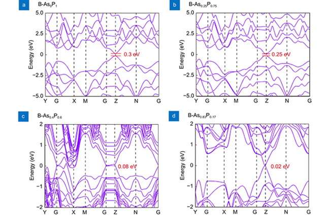
    Fig. 2. Band gap structures of the B-AsxP1-x with different value of “x” (x = 0, 0.25, 0.4, and 0.83).
    (a) The band gap structure of the B-AsxP1-x (x = 0.4) NSs. (b) The 2D B-AsP NSs dispersions used in our experiment, and the Tyndall effect observed as the laser beams transmitted through the sample. (c) The phase-shift of the incident light caused by the Kerr nonlinearity in 2D B-AsP NSs. (d) Experimental schematic of the SSPM based on the 2D B-AsP NSs dispersions. (e, f) The intensity-dependent diffraction patterns generated from the 2D B-AsP NSs dispersions with the lasers of λ = 532 nm and 671 nm, respectively. (g, h) The nonlinear optical response (R) for the 2D B-AsP NSs dispersions with three repeated measurements at λ = 532 nm and 671 nm, respectively.
    Fig. 3. (a) The band gap structure of the B-AsxP1-x (x = 0.4) NSs. (b) The 2D B-AsP NSs dispersions used in our experiment, and the Tyndall effect observed as the laser beams transmitted through the sample. (c) The phase-shift of the incident light caused by the Kerr nonlinearity in 2D B-AsP NSs. (d) Experimental schematic of the SSPM based on the 2D B-AsP NSs dispersions. (e, f) The intensity-dependent diffraction patterns generated from the 2D B-AsP NSs dispersions with the lasers of λ = 532 nm and 671 nm, respectively. (g, h) The nonlinear optical response (R) for the 2D B-AsP NSs dispersions with three repeated measurements at λ = 532 nm and 671 nm, respectively.
    (a) The diffraction patterns excited from the 2D B-AsP NSs dispersions with a high light intensity for consecutive 6 hours. (b) The absorption spectrums for the 2D B-AsP NSs dispersions before and after 6 hours of exposure.
    Fig. 4. (a) The diffraction patterns excited from the 2D B-AsP NSs dispersions with a high light intensity for consecutive 6 hours. (b) The absorption spectrums for the 2D B-AsP NSs dispersions before and after 6 hours of exposure.
    (a) Experimental schematic of the 2D B-AsP-based all-optical phase modulated system. (b) The phase modulation of controlling light to signal light. (c) The number of diffraction rings modulated by the intensity of controlling light. (d) Result of the all-optical switching based on 2D B-AsP NSs to realize the functions of “on” and “off”. (e) 2D B-AsP NSs all-optical logical gate to achieve the “or” function.
    Fig. 5. (a) Experimental schematic of the 2D B-AsP-based all-optical phase modulated system. (b) The phase modulation of controlling light to signal light. (c) The number of diffraction rings modulated by the intensity of controlling light. (d) Result of the all-optical switching based on 2D B-AsP NSs to realize the functions of “on” and “off”. (e) 2D B-AsP NSs all-optical logical gate to achieve the “or” function.
    The unidirectional nonlinear excitation in 2D B-AsP/ SnS2 hybrid structure to achieve the spatial asymmetric light propagation.
    Fig. 6. The unidirectional nonlinear excitation in 2D B-AsP/ SnS2 hybrid structure to achieve the spatial asymmetric light propagation.
    Leiming Wu, Taojian Fan, Songrui Wei, Yijun Xu, Ye Zhang, Dingtao Ma, Yiqing Shu, Yuanjiang Xiang, Jun Liu, Jianqing Li, Krassimir Panajotov, Yuwen Qin, Han Zhang. All-optical logic devices based on black arsenic–phosphorus with strong nonlinear optical response and high stability[J]. Opto-Electronic Advances, 2022, 5(1): 200046
    Download Citation