Abstract
![]()
![]() The Kerr nonlinearity in two-dimensional (2D) nanomaterials is emerging as an appealing and intriguing research area due to their prominent light processing, modulation, and manipulation abilities. In this contribution, 2D black arsenic-phosphorus (B-AsP) nanosheets (NSs) were applied in nonlinear photonic devices based on spatial self-phase modulation (SSPM) method. By applying the Kerr nonlinearity in 2D B-AsP, an all-optical phase-modulated system is proposed to realize the functions of “on” and “off” in all-optical switching. By using the same all-optical phase-modulated system, another optical logic gate is proposed, and the logical “or” function is obtained based on the 2D B-AsP NSs dispersions. Moreover, by using the SSPM method, a 2D B-AsP/SnS2 hybrid structure is fabricated, and the result illustrates that the hybrid structure possesses the ability of the unidirectional nonlinear excitation, which helps in obtaining the function of spatial asymmetric light propagation. This function is considered an important prerequisite for the realization of diode functionalization, which is believed to be a factor in important basis for the design of isolators as well. The initial investigations indicate that 2D B-AsP is applicable for designing optical logical devices, which can be considered as an important development in all-optical information processing.
The Kerr nonlinearity in two-dimensional (2D) nanomaterials is emerging as an appealing and intriguing research area due to their prominent light processing, modulation, and manipulation abilities. In this contribution, 2D black arsenic-phosphorus (B-AsP) nanosheets (NSs) were applied in nonlinear photonic devices based on spatial self-phase modulation (SSPM) method. By applying the Kerr nonlinearity in 2D B-AsP, an all-optical phase-modulated system is proposed to realize the functions of “on” and “off” in all-optical switching. By using the same all-optical phase-modulated system, another optical logic gate is proposed, and the logical “or” function is obtained based on the 2D B-AsP NSs dispersions. Moreover, by using the SSPM method, a 2D B-AsP/SnS2 hybrid structure is fabricated, and the result illustrates that the hybrid structure possesses the ability of the unidirectional nonlinear excitation, which helps in obtaining the function of spatial asymmetric light propagation. This function is considered an important prerequisite for the realization of diode functionalization, which is believed to be a factor in important basis for the design of isolators as well. The initial investigations indicate that 2D B-AsP is applicable for designing optical logical devices, which can be considered as an important development in all-optical information processing.Introduction
The all-optical modulation technology is considered an emerging research field that may have a significant impact in the future. As compared to the conventional electrical modulation technology, the most prominent advantage of the all-optical modulation technology is its fast speed and strong anti-interference ability. Especially in a complex electromagnetic environment, the electrical modulation technology is considered more susceptible to interference, which adversely affects the modulation signal. In order to solve the deficiency of the traditional electro-optical and optoelectronic modulation technologies, the all-optical modulation technology1-4 is developed for designing new photonic devices5-8, so that information can always be processed in an optical approach, which thus ignores the disadvantages. The SSPM and spatial cross-phase modulation (SXPM) methods are considered interesting nonlinear optical phenomena, which are demonstrated to have a promising application in an all-optical technology7, 8.
The SSPM and SXPM are considered the optical phenomena of the Kerr effect, which are developed from the nonlinear materials, and the 2D materials are considered the representative candidates. In recent years, the number of 2D atomic materials has been increasing, and the research methods have begun to diversify. The SSPM method is also developed as an effective method for studying the optical nonlinearity of new materials. Ji et al. studied the effect of gravity on the SSPM effect of carbon nanotubes9. Wu et al. used the SSPM for studying the optical nonlinear coherence behavior of graphene material over a wide band10. Wang et al. applied the SSPM to study the tunable method for the nonlinear effect of 2D graphene at a wavelength of 632.8 nm11. Moreover, the SXPM method based on two-color lasers is also proposed to apply in the all-optical switching. Zhao et al. innovatively used the 2D MoS2 as an intermediate medium for the modulation of different lasers to achieve light-controlled light, which establishes the foundation for the application of all-optical switching based on SXPM method8. However, the applications of the SSPM and SXPM based on 2D materials are still in their infancies, and more investigations are urgently required to enrich the applications.
2D black phosphorus (BP), a fascinating 2D elemental material, has attracted adequate attention in the field of science and technology in recent years due to its remarkable physical and chemical properties. BP possesses high carrier mobility of 1,000 cm2 V−1 s−112, a large “on/off” current ratio of 10413, and a tunable band gap in the range of (0.3 eV−2.0 eV)14, which exhibits an appealing application potential in not only nanoelectronic devices, but also in nanophotonic devices such as random access memory15, 16, all-optical signal processing17, 18, phototherapy19, 20, solar cells21, 22 and highly sensitive sensors23, 24, etc. In addition, BP exhibits a strong nonlinear response so that its third-order nonlinear susceptibility is measured to be 10−8 (e.s.u.) based on the SSPM method25, and it can be applied in the all-optical technology17, 26. However, BP demonstrates an unfavorable obstacle, namely, poor stability27, 28, in practical applications. In the air environment or the aqueous solution, BP easily reacts with oxygen, thereby weakens its photoelectric properties28, 29. In order to resolve the instability defect of BP, many methods for improving stability have been reported in recent years, including metal-ion modification30, fluorination31, ligand surface coordination32, etc. Despite these promising developments, it is still challenging to simultaneously obtain high stability and retain performance similar to BP. Very recently, a substitute doping method, by adding some non-metallic atoms of As to BP to replace parts of the phosphorus atoms, has been proposed to improve the stability of BP, and then the new material of B-AsP is synthesized33. B-AsP, a derivative of phosphide 2D material, can be expressed in the form of B-AsxP1−x, where “x” in the range of 0−0.8334. By varying the value of “x”, the band gap of B-AsP can be modulated to have a broadband light–matter interaction. Moreover, 2D B-AsP also possesses the properties of a fast photoresponse and a low dark noise in order to find an application in mid-wave infrared photoconductors34-36. However, the research on 2D B-AsP is still in its infancy, and there are many physical and chemical properties and applications that are required to be explored. Especially the optical nonlinearity in 2D B-AsP has not been studied so far. In this investigation, the nonlinear properties of 2D B-AsP are studied by applying the SSPM method to realize the device functions. B-AsP is demonstrated to have a stronger nonlinear optical response than the BP, and a better optical stability as well. Considering the advantages of the high stability and the strong Kerr nonlinearity, the new 2D B-AsP material is well applied in the SSPM-based nonlinear switching, logical gate, and isolator.
Fabrication and characterizations of 2D B-AsP
The 2D B-AsP NSs used in our experiment were fabricated by using the B-AsxP1–x crystals (x= 0.4) based on the method of liquid-phase exfoliation. First, 200 mg of the B-AsP crystal was added to 200 mL of isopropanol (IPA), and a probe sonication with a power of 200 mW was used to exfoliate 2D B-AsP for 8 hours. Hereafter, the obtained B-AsP suspension was sonicated in a water bath overnight under the power of 400 W, and the temperature is maintained to below 20 °C. After applying the probe sonication and the bath sonication successively, the resultant B-AsP suspension was then centrifuged at 3000 rpm for 20 minutes. Finally, the supernatant of 2D B-AsP was extracted for further high-speed centrifugation (12000 rpm, 20 min), and 2D B-AsP was used as eventually separated sediment in our experiments. The synthesis process of B-AsP crystals is discussed in Experimental section.
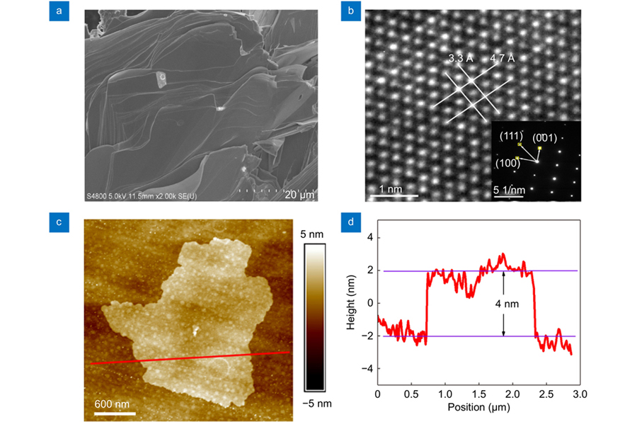
The resultant delaminated B-AsP was characterized by the scanning electron microscope (SEM) image, as shown in Fig. 1(a), which reveals a crystal structure of layered B-AsP nanomaterials. Figure 1(b) shows the orthorhombic crystal structure of B-AsP nanomaterials by the high-resolution TEM (HRTEM) image, and the interplanar spacing of lattice fringes for B-AsP is observed to be 3.3 Å and 4.7 Å (1 Å=10−10 m) in the zigzag and armchair directions, respectively. In the pattern of the selected area electron diffraction (SAED) (the inset image in Fig. 1(b)), the (100), (001) and (111) facets correspond to lattice constants of 3.3 Å, 4.7 Å and 5.8 Å, which demonstrates the high crystalline quality of the fabricated 2D B-AsP. Figure 1(c) and 1(d) display an atomic-force microscopy (AFM) image of 2D B-AsP with a thickness of 4 nm. Moreover, the band gap structure of the B-AsxP1-xnanomaterial was also investigated by using the first-principles approach (Fig. 2). When the value of “x” is “0”, the direct band gap of B-As0P1 is calculated to be ≈ 0.3 eV at the Z point (Fig. 2(a)), which well matches with previous theoretical and experimental investigations37-39. However, with the arsenic concentration increasing to a larger value, the band gap structure of the B-AsxP1–x will be destroyed and modulated to a narrow value (Figure 2(b–d)). It is worth noting that the B-AsxP1–x exhibits the characteristic of a metal conductor when x > 0.4 ( Fig. 2(c) and 2(d)).

Figure 1.(a) The SEM image of the layered B-AsP. (b) The high resolution TEM (HRTEM) image and the selected area electron diffraction (SAED) pattern of the 2D B-AsP. (c) The AFM image of 2D B-AsP. (d) The height profiles along the red line in (c).
Figure 2.Band gap structures of the B-AsxP1-x with different value of “x” (x = 0, 0.25, 0.4, and 0.83).
Calculations are performed in the density functional theory (DFT) framework as implemented in the Vienna ab initio simulation package (VASP)40. Exchange correlation energies were treated by using the generalized gradient approximation method with the Perdew-Burke-Ernzerhof function41. The projector-augmented wave42 potential was used to describe the ion-electron interaction, and the plane wave cutoff energy was set as 450 eV. The Brillouin zone of the k-point meshes was set to 13 × 9 × 7, 13 × 9 × 7, 10 × 7 × 1, 3 × 7 × 5 for pure black-P, As0.25P0.75, As0.4P0.6 and As0.83P0.17, respectively. All structures are optimized until the force of each atom converged to 0.02 eV/Å. The convergence criterion for energy was set as 10−5 eV in relaxation and set as 10−6 eV in the static calculation.
Results and discussions
Nonlinear optical response of 2D B-AsP NSs
Figure 2 shows the theoretical results of band gap structure of B-AsxP1–x with different arsenic concentrations, and the result demonstrates that the band gap of B-AsxP1–x (x = 0.4) NSs used in our experiment is 0.08 eV (Fig. 3(a)), which is similar to metals. In the following discussion, B-AsxP1–x (x = 0.4) is abbreviated as B-AsP. The light sources with the wavelengths of λ = 532 nm and 671 nm used in the experiment system are beyond the band gap, which indicates that the electrons in the valence band (VB) can be excited into the conduction band (CB) (Fig. 3(d)) due to the good light-matter interaction in the B-AsP NSs dispersions. An obvious Tyndall effect is observed as the light sources transmit through the sample (Fig. 3(b)), and then the Kerr effect in the 2D B-AsP NSs can be excited if the intensity is strong enough. The incident laser beam is a Gaussian light, which exhibits the strongest intensity at the center, and then gradually weakens toward the surrounding. The 2D B-AsP NSs are considered the intensity-dependent nonlinear materials so that the distribution of different intensities in the Gaussian spot will produce different phase-shift (Δψ) when the Gaussian light passes through the 2D B-AsP NSs, and the phase-shift distribution is considered a Gaussian-like curve (Fig. 3(c)). In the phase-shift curve, two points (r1 and r2) with the same slope can be obtained, which illustrates that the phenomenon of interference will occur due to the same wave vector ((dΔψ/dr)r1 = (dΔψ/dr)r2). The phase-shift ofr1 and r2 meet the interference condition of Δψ(r1)– Δψ(r2) = Mπ, where M is an integer (odd or even), and hence the corresponding dark or bright stripes can be achieved, respectively. Hereafter, the pattern of diffraction rings is obtained on a black screen beyond the sample, which is the so-called SSPM43.
Figure 3.(a) The band gap structure of the B-AsxP1-x (x = 0.4) NSs. (b) The 2D B-AsP NSs dispersions used in our experiment, and the Tyndall effect observed as the laser beams transmitted through the sample. (c) The phase-shift of the incident light caused by the Kerr nonlinearity in 2D B-AsP NSs. (d) Experimental schematic of the SSPM based on the 2D B-AsP NSs dispersions. (e, f) The intensity-dependent diffraction patterns generated from the 2D B-AsP NSs dispersions with the lasers of λ = 532 nm and 671 nm, respectively. (g, h) The nonlinear optical response (R) for the 2D B-AsP NSs dispersions with three repeated measurements at λ = 532 nm and 671 nm, respectively.
The diffraction patterns generated from the SSPM, which is caused by the Kerr nonlinearity in 2D B-AsP NSs, are sensitive to the intensity changes of incident laser beams. With the increasing incident intensity, a stronger nonlinear optical response will be excited to generate more diffraction rings (Fig. 3(e) and 3(f)). The nonlinear optical response (R) is defined as R = N/I10, 44, where N and I are the number of diffraction rings and the incident intensity, respectively. After the measurement, the R of 2D B-AsP is identified (Fig. 3(g) and 3(h)). Herein, the R of 2D B-AsP NSs dispersions (0.0025 mg/mL) is measured in triplicate at λ = 532 nm and 671 nm, respectively. The results demonstrate that the R of the sample at λ = 532 nm and 671 nm is approximately equal to 0.25 and 0.18, respectively, with high repeatability. Moreover, the R of the B-AsP material also has a dependence on concentration. When the concentrations of B-AsP are C1 = 0.0025 mg/mL and C2 = 0.0050 mg/mL, the corresponding values of R are 0.258 cm2/W and 0.501 cm2/W, which demonstrates that after the concentration of the B-AsP material is doubled, the corresponding nonlinear response is also nearly doubled accordingly (
Fig. S1 of the Supplementary information).
The optical stability of the 2D B-AsP NSs dispersions are also be characterized in Fig. 4. A strong enough 671 nm laser beam with a fixed intensity passes through the sample for a consecutive 6 hours, and the changes of diffraction rings are recorded in real time by a camera. The diffraction patterns are shown in Fig. 4(a) for every hour, which illustrates that the 2D B-AsP NSs dispersions possess a good optical stability under the exposure of strong incident light. The absorption spectra of the 2D B-AsP NSs dispersions before and after 6 hours of exposure are shown in Fig. 4(b). Only a slight change in absorption spectra is measured, which hardly affects the experimental results. The nonlinear optical response of BP and B-AsP is shown in
Figure S2 of the Supporting Information. The nonlinear refractive index and the third-order nonlinear susceptibility of B-AsP can be obtained as: , and (the λ, n0, and Leff are the wavelength, linear refractive index, and effective optical thickness of materials)8, which indicates that the n2 andχ(3) are proportional to N/I (nonlinear optical response). Previous report25 indicates that the nonlinear refractive index and the third-order nonlinear susceptibility of BP at the wavelength range of 350–1160 nm are measured to be n2 ~10−5 cm2/W and χ(3) ~10−8. In this work, the nonlinear optical response of 2D B-AsP is measured and compared with BP (
Fig. S2 of the Supplementary information). The result indicates that the nonlinear optical response of B-AsP is slightly larger than that of BP, and this means that the χ(3) of B-AsP is approximately ~10−8, similar to BP.
Figure 4.(a) The diffraction patterns excited from the 2D B-AsP NSs dispersions with a high light intensity for consecutive 6 hours. (b) The absorption spectrums for the 2D B-AsP NSs dispersions before and after 6 hours of exposure.
2D B-AsP-based all-optical phase modulated system
By using the Kerr nonlinearity in the 2D B-AsP, a 2D B-AsP-based all-optical phase-modulated system (Fig. 5(a)) is proposed based on the SXPM method to realize light-to-light modulation. Normally, when two beams of light meet in space, they do not interact with each other, and continue to propagate along their respective directions. However, this phenomenon fails if the lights meet in the 2D B-AsP NSs dispersions. The nonlinear material of 2D B-AsP NSs has the ability to modulate the phase of incident lights. When the incident lights are beyond the band gap of 2D B-AsP NSs and their intensities are strong enough, the SSPM will be excited. The SXPM refers to the mutual modulation of the phase between two laser beams, including a controlling light and the other signal light. First of all, the 532 nm green laser beam is selected as the signal light, which is modulated to a low intensity (< 4 W/cm2), which is well below the excitation threshold of the nonlinear optical response (Fig. 5(b–1)). Therefore, the other controlling light (671 nm red light) with strong enough intensity is incorporated into the optical path by using a beam splitter (BS), and then the diffraction rings of the controlling light are excited. More interestingly, the diffraction pattern of the signal light (green light) is also induced, and the number of diffraction rings is increased with an increase in the controlling light intensity (Fig. 5(b)). When the controlling light passes through the sample, the refractive index of B-AsP NSs changes due to the Kerr effect, which then inversely modulates the phase of the incident light. According to the SXPM method, the light field of the signal light will be promoted by the controlling light in order to enhance the phase-shift, which further generates the diffraction rings.
Figure 5.(a) Experimental schematic of the 2D B-AsP-based all-optical phase modulated system. (b) The phase modulation of controlling light to signal light. (c) The number of diffraction rings modulated by the intensity of controlling light. (d) Result of the all-optical switching based on 2D B-AsP NSs to realize the functions of “on” and “off”. (e) 2D B-AsP NSs all-optical logical gate to achieve the “or” function.
The number of diffraction rings of the signal light (λ = 532 nm) modulated by the intensity of controlling light (λ = 671 nm) is shown in Fig. 5(c). The R of the signal light is found to be approximately equal to 0.18, which similar to the R of the 671 nm laser beam measured in Fig. 3(h). The 2D B-AsP-based all-optical phase-modulated system exhibits good application prospect in the all-optical switching. In the modulated system, both the signal light and controlling light are set to a fixed intensity so that the controlling light has a strong intensity (45.32 W/cm2), whereas the intensity of the signal light has a low value (3.76 W/cm2). When the controlling light is set to the “ON” mode, the number of diffraction rings of the signal light will be induced to be 8; when the controlling light is set to the “OFF” mode, the number of diffraction rings of the signal light will be induced to be 1 (Fig. 5(d)). The “excitation” and the “non-excitation” of the diffraction rings in the signal light can be considered as the “on” and “off” instructions in the B-AsP-based all-optical switching.
Moreover, taking advantage of the all-optical phase-modulated system, another 2D B-AsP-based all-optical logical gate is proposed to realize the function of “or” gate. The “or” gate possesses four sub-functions, namely, “0 + 0 = 0”, “0 + 1 = 1”, “1 + 0 = 1”, and “1 + 1 = 1”. Normally, the “or” gate is implemented by electricity, and here we have proposed an all-optical pathway of using 2D B-AsP to realize the logical function of the “or” gate. In our all-optical phase-modulated system, “Laser A” and “Laser B” are the input signals, and “Y = Laser A + Laser B” is the output signal. The “excitation” and the “non-excitation” of the diffraction rings are represented by the output signals in a high level of “1” and a low level of “0”, respectively. First, both “Laser A” and “Laser B” are modulated below the threshold so that the diffraction rings cannot be excited, and the inputs are two low-level signals of “0” (Fig. 5(e)-(1, 2)). By using the 2D B-AsP-based all-optical phase modulated system, these two input signals are processed, and the output signal (Y) is also at a low level of “0” (Fig. 5(e)-(3)). Second, if the “Laser A” is set at a low level of “0”, whereas“Laser B” is set at a high level of “1”, the output signal will become a high level of “1” (Fig. 5(e)-(4–6)). Third, if “Laser A” and “Laser B” are set at a high level of “1” and a low level of “0”, respectively, the output signal of “Y” will reveal a high level of “1” (Fig. 5(e)-(7–9)). Form Fig. 5(e)-(4–6) and Fig. 5(e)-(7–9), it can be observed that the diffraction rings excited by different wavelengths can be modulated with each other. Fourth, when both “Laser A” and “Laser B” are capable of generating the diffraction rings in a high level of “1”, the output signal will still maintain a high level of “1” (Fig. 5(e)-(10–12)).
Spatial asymmetric light propagation in 2D B-AsP
In this section, we describe a hybrid structure that enables spatial asymmetric light propagation (namely non-reciprocal light propagation). 2D B-AsP is demonstrated to possess a strong nonlinear optical response with a narrow band gap of 0.08 eV (Fig. 3(a)), which displays a potential application in photonic devices. In order to realize the ability of spatial asymmetric light propagation in a photonic diode or an isolator, an auxiliary material of 2D SnS2 is introduced and combined with 2D B-AsP to form a hybrid structure. 2D SnS2 is a reverse saturable absorption (RSA) material45, which possesses a large band gap (Eg = 2.6 eV)46. The light sources used in our experiment are within the band gap of SnS2 so that the ability of light-matter interaction requires two-photon absorption to achieve the excitation of electrons at the VB into the CB. In the experiment of the SSPM, the Kerr effect of the 2D material is used instead of the saturated absorption effect. For the excitation of the Kerr nonlinearity in 2D B-AsP only a relatively low intensity is required, and the low intensity is found not strong enough to support the two-photon absorption behavior in 2D SnS2. When the laser beams pass through SnS2 dispersions, the light-matter interaction does not occur so that the diffraction rings cannot be excited.
Herein, the 2D B-AsP and SnS2 dispersions are respectively filled in two quartz cuvettes that are closed together to form a hybrid structure (Fig. 6). When a laser beam (λ = 671 nm) passes through in the positive direction (B-AsP/ SnS2), the light first interacts with the sample of 2D B-AsP NSs to excite the Kerr effect and further generate the diffraction rings. Thereafter, the light spot forming the diffraction rings will continue to pass through the second part of the 2D SnS2 material. In 2D SnS2 dispersions, the number of rings does not change since there is no interaction between light and SnS2, but the light intensity is weakened due to the linear absorption. Finally, we can observe that the diffraction rings are generated in a positive direction. Conversely, if the laser beam passes through in the opposite direction (SnS2/ B-AsP), the light first interacts with the SnS2 material, but the diffraction rings cannot be excited and the intensity is weakened by the linear absorption. Thereafter, the weakened light continues to pass through the sample of B-AsP dispersions. However, the light intensity is seriously weakened, which is found to be lower than the threshold of the excited Kerr nonlinearity in 2D B-AsP, and the diffraction rings cannot be generated, hence only a light point can be obtained from the opposite direction. The unidirectional nonlinear excitation in the 2D B-AsP/ SnS2 hybrid structure is considered an important prerequisite for the realization of diode functionalization as well as the design of isolators in order to obtain the spatial asymmetric light propagation. This phenomenon of the unidirectional nonlinear excitation can be obtained not only at λ = 671 nm, but also at λ = 532 nm (
Figure S3, Supplementary information), which indicates that the hybrid structure shows a broadband optical response to realize the spatial asymmetric light propagation.
Figure 6.The unidirectional nonlinear excitation in 2D B-AsP/ SnS2 hybrid structure to achieve the spatial asymmetric light propagation.
Conclusion
In this work, we have successfully fabricated a new 2D material, namely, 2D B-AsP NSs, the band gap of which is calculated to be 0.08 eV. In addition, the morphology, size, and lattice distance of the 2D B-AsP NSs are also characterized. Thereafter, we have explored the nonlinear optical properties of the B-AsP nanomaterial and applied it in the design of photonic devices. First, by using the SSPM method, the nonlinear optical response of 2D B-AsP NSs is measured in a broadband with a high optical stability. Second, a 2D B-AsP-based all-optical phase-modulated system based on the SXPM method is proposed in order to obtain the modulation of the controlling light to the signal light. Depending on the phase-modulated system, an all-optical switching is designed to realize the functions of “on” and “off” based on the Kerr nonlinearity in 2D B-AsP. Moreover, based on the same phase-modulated system, another optical logical gate that possesses the “or” function is proposed. Third, a hybrid structure consisting of 2D B-AsP and SnS2 is explored by using the SSPM method, and the results demonstrate that the hybrid structure is able to generate the effect of the unidirectional nonlinear excitation, breaking the spatial light reversible propagation, which provides a feasible solution to the design of the photonic diodes or the optical isolators.
Experimental section
The mineralizer-assisted chemical vapor transport (CVT) method was used to fabricate high-quality B-AsP. The precursors used in the experiment were gray arsenic and red phosphorus (molar ratio, 4∶6), and the total mass was 500 mg. The precursor and the 10 mg mineralization agent (tin iodide, SnI4) were placed horizontally in a vacuum quartz tube and sealed by the Partulab device (MRVS-1002). The furnace was heated to 750 °C at a rate of 5 °C/min and maintained for 2 hours. Then, the furnace was cooled to 500 °C for 7.5 hours and maintained for 3 hours. After slowly cooling to 150 °C for 8 hours, the furnace was cooled to room temperature. Then the B-AsP crystals can be obtained at the cold end of the tube.
The scanning electron microscope (SEM, Quanta FEG 250) was used to investigate the morphology of B-AsP NSs. The transmission electron microscope (TEM) image and the SAED pattern were obtained from a Tecnai G2 F20 S-TWIN (field-emission) scanning transmission electron microscope operating at 200 kV. Atomic-force microscopy (AFM, BRUKER Dimension ICON, 512 pixels per line) was used to determine the thickness and the morphology of 2D B-AsP. The sample for the AFM measurement was prepared by dispersing 2D B-AsP into IPA and dropping it onto Si/SiO2 substrates.