Yongjiu Yuan, Xin Li. Femtosecond Laser Processing of Graphene and Its Application[J]. Laser & Optoelectronics Progress, 2020, 57(11): 111414
Search by keywords or author
- Laser & Optoelectronics Progress
- Vol. 57, Issue 11, 111414 (2020)
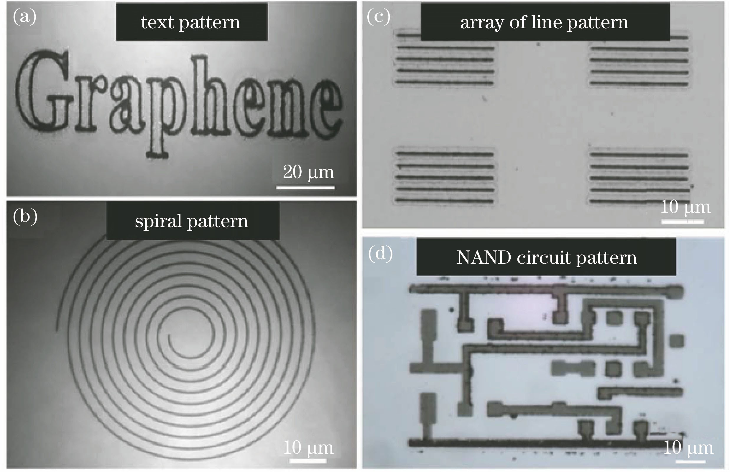
![Micro-nano structure of graphene film. (a) Graphene text pattern on a glass substrate; (b) graphene spiral pattern on a glass substrate; (c) arrays of graphene lines on a glass substrate; (d) circuit pattern on a SiO2/Si substrate[22]](/richHtml/lop/2020/57/11/111414/img_1.jpg)
Fig. 1. Micro-nano structure of graphene film. (a) Graphene text pattern on a glass substrate; (b) graphene spiral pattern on a glass substrate; (c) arrays of graphene lines on a glass substrate; (d) circuit pattern on a SiO2/Si substrate[22]
![Experimental results. (a) Optical images of CW laser irradiated spots at various laser powers[31]; (b) SEM and AFM images of periodic surface structures[32]](/richHtml/lop/2020/57/11/111414/img_2.jpg)
Fig. 2. Experimental results. (a) Optical images of CW laser irradiated spots at various laser powers[31]; (b) SEM and AFM images of periodic surface structures[32]
Fig. 3. Schematics illustration of the procedures to produce the graphene flower using femtosecond laser pulses[34]. (a) Graphene oxide sheets; (b) reduced graphene sheets; (c) graphene film by filtration of reduced graphene sheets; (d) a graphene microflower produced with a single laser pulse; (e) large-area surface patterning by fs laser direct writing; (f) large-area uniform flower patterns on the surface of a graphene film
Fig. 4. Experimental results.(a) TEM and AFM images of N-GQDs[43]; (b) TEM image of graphene oxide sheets after 30 min of laser ablation[44]
Fig. 5. Experimental results. (a) Preparative scheme of graphene oxide film; (b)-(d) optical microscopy images of different graphene patterns processed[45]
Fig. 6. Process flow of the laser-induced pattern transfer method[48]
Fig. 7. Femtosecond laser fabricates interdigitated capacitor on graphene film[53].(a) Flow chart of preparation process; (b)-(f) photomicrograph and enlarged view of processed micro-supercapacitors

Set citation alerts for the article
Please enter your email address


