Abstract
The instability of lead halide perovskites in various application-related conditions is a key challenge to be resolved. We investigated the formation of metal nanoparticles during transmission electron microscopy (TEM) imaging of perovskite-related metal halide compounds. The metal nanoparticle formation on these materials originates from stimulated desorption of halogen under electron beams and subsequent aggregation of metal atoms. Based on shared mechanisms, the TEM-based degradation test can help to evaluate the material stability against light irradiation.1. Introduction
Halide perovskites, a class of materials with chemical formula of [where A is an organic type like methylammonium (MA, ) and formamidinium (FA, ) or inorganic like Cs, B is or Sn, X is , Br, or I], possess superior optoelectronic properties and therefore have attracted tremendous attention in the fields of photovoltaics, photodetection, light emitting diodes, scintillation, and photocatalysis[1–10]. Despite the enhanced stability of the all-inorganic halide-perovskite-based devices compared to the hybrid ones[11–13], the degradation of all-inorganic halide perovskites under the action of external stimuli like UV light is still inevitable and presents as an obstacle towards stable device performances. UV light soaking all-inorganic perovskite nanocrystals such as suffer from the merging and aggregation of nanocrystals into larger particles and additional introduction of trap states[14,15]. Considering that such nanocrystals are mostly reported to be terminated with CsBr, and part of the Cs ions are substituted with ligand[16–18], their predominant merging into a continuous perovskite lattice under UV illumination indicates the occurrence of ion migration at the boundaries of adjacent nanocrystals and even the desorption of bromine. Photon stimulated halogen desorption is not new for halogen containing materials and is generally driven by electronic transitions[19–21]. We postulate that electronic-transition-induced halogen desorption occurs at the nanocrystal boundaries as well in the light triggered transformation process. This effect, however, has been neglected due to the limited spatial resolution of optical spectroscopic measurements.
Fortunately, halogen desorption is also shared in the interaction of all-inorganic halide perovskites with other excitation sources such as an energetic electron beam. Especially, the unique advantages of the superior spatial resolution of advanced transmission electron microscopy (TEM) techniques, and the versatility that this tool provides by incorporating various in-situ holders such as heating enabled more precise monitoring and profound understanding of degradation mechanisms of halide perovskites under electron beam irradiation. Numerous works on the electron-beam-induced degradation of have been reported, especially on thin films and nanocrystals[22–25]. The reported transformation is generally featured by temperature-dependent metallic lead nanoparticles formation and halogen desorption during in-situ TEM imaging and analysis.
With massive efforts in recent years, a wide range of all-inorganic perovskite-related compounds with various compositions and phases have emerged, such as , , , , and [26–29]. Similar to the standard , most of the all-inorganic perovskite-related compounds are also unstable, and it is necessary to understand their degradation pathways. Herein, following the above-mentioned works on nanocrystals, we expanded in-situ TEM investigations to the nanocrystals of and two lead-free halide-perovskite-related compounds. Intriguingly, we observed similar phenomena of temperature-dependent metal nanoparticle formation upon electron beam irradiation. Based on these observations, we extend the previously established understanding of the Pb nanoparticle creation in to the lead-free cases and propose a generalized mechanism for high-energy electron-beam-induced metal nanoparticle formation on all of the inorganic halide-perovskite-related compounds. A better understanding of the degradation mechanism of these electron-beam-sensitive halide perovskites can give intuition into the understanding of their interaction with light.
Sign up for Chinese Optics Letters TOC. Get the latest issue of Chinese Optics Letters delivered right to you!Sign up now
2. Experimental Methods
We started with synthesizing the nanomaterials of various inorganic halide-perovskite-related compounds using a hot injection colloidal synthesis approach, as reported in Refs. [27,30,31] and described in Supplementary Materials. These nanocrystals include nanocubes and nanosheets, nanocrystals, nanowires, and nanocrystals, for which the morphology and size are listed in Table S1 in Supplementary Materials. After the synthesis, the morphology, structure and composition evolution of these nanomaterials induced by the incident electron beam is investigated by using a JEOL-2200FS microscope.
3. Results and Discussion
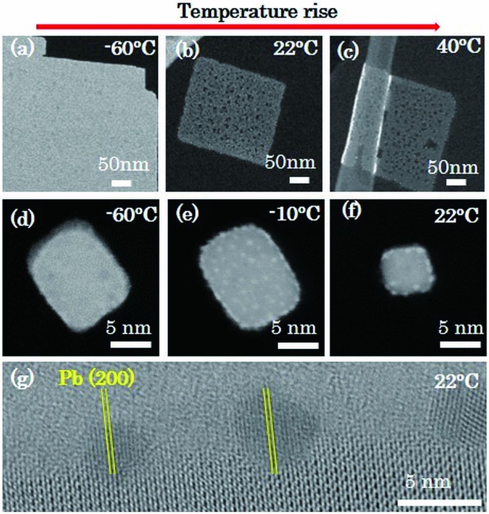
Figures 1(a)–1(f) report the high angular annular dark-field-scanning TEM (HAADF-STEM) images of nanocrystals after 200 keV electron beam irradiation at three different temperatures. Similar to our earlier work[23], a high-energy electron beam induces the transformation process of nanocrystals, in which metallic lead nanoparticles [as confirmed in the high-resolution TEM (HRTEM) analysis of Fig. 1(g)] are formed above certain temperatures. Through the composition analysis, as shown in Figs. S1, S2 and Table S2 of Supplementary Materials, we identify the mechanism as a stimulated desorption and subsequent diffusion process. Stimulated desorption is featured by the occurrence of bromine desorption and concurrent reduction of ions to species. This tandem effect of halogen desorption and reduction resembles the stimulated desorption that occurs in the TEM study of and some oxides (such as CuO, , , )[32–36]. One stimulated desorption pathway is based on a Knotek–Feibelman inter-atom Auger mechanism[37,38], in which an inner-shell electron of the cation (i.e., ) is excited by an incident electron, creating an inner-shell hole; the electron from an adjacent anion (i.e., ) fills this vacancy. The energy released is absorbed by other electrons of the anion, leading to Auger emission. Consequently, the anion species are oxidized to a neutral or cation state (i.e., to or ) and then migrate to the surface and are desorbed to the vacuum. Meanwhile, the Pb ions are reduced to . Therefore, the stimulated desorption process of all-inorganic halide perovskite can be mainly defined as a type of ionization damage[39].

Figure 1.HAADF-STEM images demonstrating the Pb nanoparticle formation on CsPbBr3 nanocrystals induced by 200 keV electron irradiation at increasing temperature: (a)–(c) 3 nm thick nanosheet and (d)–(f) nanocubes of edge size of 20 nm. (g) HRTEM image of CsPbBr3 nanosheet showing the atomic details of the Pb nanoparticles.
Additionally, the overall damage process also involves knock-on displacement because the incident electrons can transfer momentum to both the loosened bromine species and the reduced lead species and consequently speed up their diffusion process. As a consequence, Pb nanoparticle formation is influenced by the incident electron energy in a complex way: on one hand, the radiolysis damage is less pronounced at higher incident electron energy; on the other hand, higher-energy electrons cause more significant knock-on displacement that enhances both the oxidized bromine desorption and the atom diffusion. We compared composition change induced by electrons of two energies (80 keV and 200 keV) and found that the overall damage is less pronounced at higher energy, suggesting the dominance of ionization damage mechanisms (see Fig. S3 of Supplementary Materials).
Since the diffusion process depends largely on the substrate temperature, with rising temperatures, an obvious increase in the number and size of Pb nanoparticles is observed in Fig. 1. Two mechanisms are at work simultaneously here: (1) a faster thermally activated diffusion of the oxidized bromine species leads to a faster stimulated desorption process and production of more species; (2) the promotion of diffusion and aggregation of atoms gives rise to more and larger Pb nanoparticles.
We have also examined the transformation of another lead-based and two lead-free perovskite-related halide compounds under an electron beam. is a lead-based perovskite-related compound that has a crystal structure, in which octahedra are disconnected, as illustrated in Fig. 2(a). The HAADF-STEM images of hexagonal shape nanocrystals with an edge size of taken at , 22, and 45°C are displayed in Figs. 2(b), 2(c), and 2(d), respectively. Upon electron exposure, no distinguishable Pb nanoparticle forms at , while particles with appreciable size and contrast, as labelled by the yellow arrows, start appearing at 22°C, and the size increases further at 45°C.
Figure 2.Crystal model and HAADF-STEM images at different temperatures under 200 keV electron irradiation for nanocrystals of (a)–(d) Cs4PbBr6 (Cs, Br, and Pb atoms as big cyan spheres, small green and blue spheres, respectively, PbBr6 octahedra are shaded in blue), (e)–(h) Cs3CoCl5 (Cs atoms in cyan, Cl atoms in green, Co atoms in blue, CoCl6 octahedra in blue), (i)–(k) Cs3Bi2I9 (Cs atoms in cyan, I atoms in green, Bi atoms in blue, and BiI6 octahedra in blue).
is a type of lead-free halide-perovskite-related compound, which has a lattice structure shown in Fig. 2(e). The HAADF-STEM images of the as synthesized nanowires of 5–8 nm in width at various temperatures are displayed in Figs. 2(f)–2(h). No nanoparticle is observed at 22°C, but, when the temperature is raised to 130°C, bright nanoparticles start emerging. The size and number of these nanoparticles increase further when imaged at 170°C. More experimental data of those lead-free compounds are presented in Fig. 3. The HRTEM images in Figs. 3(a) and 3(b) reveal that the nanoparticles on are made of Co, and their lattice structure is cubic, which is a metastable phase for Co. Besides brighter nanoparticles, one may also notice that the nanowires have merged laterally and broken into short pieces, as shown in Fig. 2(h).
Figure 3.HRTEM images of (a), (b) Cs3CoCl5 nanowires showing the formation of metallic Co nanoparticles and (c), (d) Cs3Bi2I9 naoncrystals demonstrating the creation of Bi nanoparticles.
, a Bi-based perovskite-related halide, has the lattice shown in Fig. 2(i). When irradiated with a 200 keV electron beam at 22°C, nanoparticles are already observable, as shown in Fig. 2(j), indicating a high sensitivity of to the electron beam. A rise in temperature also causes coarsening of the nanoparticles, so fewer nanoparticles are observed in Fig. 2(k), which was imaged at 50°C. We have analyzed the nature of these nanoparticles based on the HRTEM images shown in Figs. 3(c) and 3(d) and found that their structure matches with the tetragonal phase of metallic Bi. It is noted that the number of Bi nanoparticles decreases at 50°C, indicating that the radiolysis is an easy process for , so electron irradiation at 22°C can already induce prominent radiolysis effect, and an increase in temperature only facilitates a faster diffusion of the formed metallic species. The fast diffusion of Bi is probably related to its low melting point as well.
The similarity shared by the atomic structure of these metal halide-perovskite-related compounds is that the compound involves coordination of metal M (M can be Co, Bi, or Pb) and halogen X (i.e., X is , Br, or I) into an octahedron. As shown in the above TEM data, although the metal nanoparticle formation rate and the temperature to render visible nanoparticle formation in TEM imaging are different for various compounds, the same phenomenon of a temperature-dependent high contrast nanoparticle formation is observed under high-energy electron beam irradiation. Our results suggest that a temperature-dependent nanoparticle formation occurs for all of these compounds under high-energy electron irradiation in the TEM imaging process. Similar evolution of these materials under electron irradiation suggests some common features in the atomic and electronic structures and their interaction mechanism with energetic electrons. We are investigating these issues further in our future studies.
The underlying mechanisms that lead to metal cation reduction in metal halide perovskites exposed to light (including UV) and electron beam can be compared. The photons with energy larger than the bandgap mainly generate hot electrons and holes[12], which promote chemical bond breaking in the perovskites and stimulate desorption of loosely binding species near the surface. Such hot carriers are also generated (indirectly in most cases[40]) by the energetic electron beam in TEM imaging, with similar consequences. The rate of material degradation under the electron beam seems to be much faster and more dramatic than that of photon exposure. Therefore, TEM-based degradation analysis could serve the purpose of burn-in tests for the stability of the perovskites against photon and hot carrier damages[22,41] at a high spatial resolution. Of course, energetic electrons can induce damages also through the knock-on and core-level electron excitation, followed by inter-atomic Auger processes, which are unlikely by photons. Further investigations are needed in order to employ TEM-based analysis for accurate evaluation of the stability of these materials exposed to photons or hot carriers.
4. Conclusion
In summary, our in-situ TEM investigation demonstrates that the instability of metal halide-perovskite-related compounds under high-energy electron irradiation is universal. This degradation process is generally featured by the desorption of halogen species and emergence of metal nanoparticles, which are the combined results of predominant ionization damage and subsidiary knock-on displacement effects. The observed universal phenomenon of electronic transition driven halogen desorption in TEM may also occur when the material is exposed to UV light. Based on a clear understanding of the similarity and difference between the materials degradation processes under electron and photon beams, TEM-based analysis can be used to characterize quickly the material instability against photon damage with a nanoscale resolution.
References
[1] Z. Lian, Q. Yan, Q. Lv, Y. Wang, L. Liu, L. Zhang, S. Pan, Q. Li, L. Wang, J. L. Sun. High-performance planar-type photodetector on (100) facet of MAPbI3 single crystal. Sci. Rep., 5, 16563(2015).
[2] Q. Chen, J. Wu, X. Ou, B. Huang, J. Almutlaq, A. A. Zhumekenov, X. Guan, S. Han, L. Liang, Z. Yi, J. Li, X. Xie, Y. Wang, Y. Li, D. Fan, D. B. L. Teh, A. H. All, O. F. Mohammed, O. M. Bakr, T. Wu, M. Bettinelli, H. Yang, W. Huang, X. Liu. All-inorganic perovskite nanocrystal scintillators. Nature, 561, 88(2018).
[3] Y.-H. Kim, G.-H. Lee, Y.-T. Kim, C. Wolf, H. J. Yun, W. Kwon, C. G. Park, T.-W. Lee. High efficiency perovskite light-emitting diodes of ligand-engineered colloidal formamidinium lead bromide nanoparticles. Nano Energy, 38, 51(2017).
[4] Z. Chen, Y. Hu, J. Wang, Q. Shen, Y. Zhang, C. Ding, Y. Bai, G. Jiang, Z. Li, N. Gaponik. Boosting photocatalytic CO2 reduction on CsPbBr3 perovskite nanocrystals by immobilizing metal complexes. Chem. Mater., 32, 1517(2020).
[5] A. K. Jena, A. Kulkarni, T. Miyasaka. Halide perovskite photovoltaics: background, status, and future prospects. Chem. Rev., 119, 3036(2019).
[6] J. Shamsi, D. Kubicki, D. Kubicki, M. Anaya, Y. Liu, K. Ji, K. Frohna, C. P. Grey, R. H. Friend, S. D. Stranks, S. D. Stranks. Stable hexylphosphonate-capped blue-emitting quantum-confined CsPbBr3 nanoplatelets. ACS Energy Lett., 5, 1900(2020).
[7] H. Gao. Halide perovskites—an emerging class of optoelectronic materials. Light, Energy, and the Environment, PTu3B.1(2016).
[8] J. Kim, E. Kim, H. Moon, S. Yoo. Realization of foldable perovskite light-emitting diodes. OSA Advanced Photonics Congress, PvW1G.2(2020).
[9] M. Kim. Perovskite photovoltaics: the road ahead. Opt. Photon. News, 31, 32(2020).
[10] H. Fan, Y. Mu, C. Liu, Y. Zhu, G. Liu, S. Wang, Y. Li, P. Du. Random lasing of CsPbBr3 perovskite thin films pumped by modulated electron beam. Chin. Opt. Lett., 18, 011403(2020).
[11] C. Wu, Y. Zou, T. Wu, M. Ban, V. Pecunia, Y. Han, Q. Liu, T. Song, S. Duhm, B. Sun. Improved performance and stability of all-inorganic perovskite light-emitting diodes by antisolvent vapor treatment. Adv. Funct. Mater., 27, 1700338(2017).
[12] C. C. Boyd, R. Cheacharoen, T. Leijtens, M. D. McGehee. Understanding degradation mechanisms and improving stability of perovskite photovoltaics. Chem. Rev., 119, 3418(2019).
[13] L. Zhang, P. H. L. Sit. Ab initio study of the role of oxygen and excess electrons in the degradation of CH3NH3PbI3. Asia Communications and Photonics Conference, Su1H.4(2017).
[14] S. Huang, Z. Li, B. Wang, N. Zhu, C. Zhang, L. Kong, Q. Zhang, A. Shan, L. Li. Morphology evolution and degradation of CsPbBr3 nanocrystals under blue light-emitting diode illumination. ACS Appl. Mater. Interfaces, 9, 7249(2017).
[15] J. Shamsi, P. Rastogi, V. Caligiuri, A. L. Abdelhady, D. Spirito, L. Manna, R. Krahne. Bright-emitting perovskite films by large-scale synthesis and photoinduced solid-state transformation of CsPbBr3 nanoplatelets. ACS Nano, 11, 10206(2017).
[16] V. K. Ravi, P. K. Santra, N. Joshi, J. Chugh, S. K. Singh, H. Rensmo, P. Ghosh, A. Nag. Origin of the substitution mechanism for the binding of organic ligands on the surface of CsPbBr3 perovskite nanocubes. J. Phys. Chem. Lett., 8, 4988(2017).
[17] Y. Chen, S. R. Smock, A. H. Flintgruber, F. A. Perras, R. L. Brutchey, A. J. Rossini. Surface termination of CsPbBr3 perovskite quantum dots determined by solid-state NMR spectroscopy. J. Am. Chem. Soc., 142, 6117(2020).
[18] M. I. Bodnarchuk, S. C. Boehme, S. ten Brinck, C. Bernasconi, Y. Shynkarenko, F. Krieg, R. Widmer, B. Aeschlimann, D. Günther, M. V. Kovalenko, I. Infante. Rationalizing and controlling the surface structure and electronic passivation of cesium lead halide nanocrystals. ACS Energy Lett., 4, 63(2019).
[19] M. N. Kabler, R. T. Williams. Vacancy-interstitial pair production via electron-hole recombination in halide crystals. Phys. Rev. B, 18, 1948(1978).
[20] M. Szymonski, A. Droba, M. Goryl, J. J. Kolodziej, F. Krok. Alkali halide decomposition and desorption by photons—the role of excited point defects and surface topographies. J. Phys. Condens. Matter, 18, S1547(2006).
[21] R. F. Haglund, N. H. Tolk. Time-resolved laser-induced fluorescence studies of electronically induced desorption from alkali halides. International Quantum Electronics Conference, THAA2(1986).
[22] J. Ran, O. Dyck, X. Wang, B. Yang, D. B. Geohegan, K. Xiao. Electron-beam-related studies of halide perovskites: challenges and opportunities. Adv. Energy Mater., 10, 1903191(2020).
[23] Z. Dang, J. Shamsi, F. Palazon, M. Imran, Q. A. Akkerman, S. Park, G. Bertoni, M. Prato, R. Brescia, L. Manna. In situ transmission electron microscopy study of electron beam-induced transformations in colloidal cesium lead halide perovskite nanocrystals. ACS Nano, 11, 2124(2017).
[24] X. Chen, Z. Wang. Investigating chemical and structural instabilities of lead halide perovskite induced by electron beam irradiation. Micron, 116, 73(2019).
[25] Z. Dang, J. Shamsi, Q. A. Akkerman, M. Imran, G. Bertoni, R. Brescia, L. Manna. Low-temperature electron beam-induced transformations of cesium lead halide perovskite nanocrystals. ACS Omega, 2, 5660(2017).
[26] Q. Fan, G. V. Biesold-McGee, J. Ma, Q. Xu, S. Pan, J. Peng, Z. Lin. Lead-free halide perovskite nanocrystals: crystal structures, synthesis, stabilities, and optical properties. Angew. Chemie Int. Ed., 59, 1030(2020).
[27] G. M. Paternò, N. Mishra, A. J. Barker, Z. Dang, G. Lanzani, L. Manna, A. Petrozza. Broadband defects emission and enhanced ligand Raman scattering in 0D Cs3Bi2I9 colloidal nanocrystals. Adv. Funct. Mater., 29, 1805299(2019).
[28] K. Dave, M. H. Fang, Z. Bao, H. T. Fu, R. S. Liu. Recent developments in lead-free double perovskites: structure, doping, and applications. Chem. Asian J., 15, 242(2020).
[29] R. Kaiukov, G. Almeida, S. Marras, Z. Dang, D. Baranov, U. Petralanda, I. Infante, E. Mugnaioli, A. Griesi, L. De Trizio, M. Gemmi, L. Manna. Cs3Cu4In2Cl13 nanocrystals: a perovskite-related structure with inorganic clusters at A sites. Inorg. Chem., 59, 548(2020).
[30] J. Shamsi, Z. Dang, P. Bianchini, C. Canale, F. Di Stasio, R. Brescia, M. Prato, L. Manna. Colloidal synthesis of quantum confined single crystal CsPbBr3 nanosheets with lateral size control up to the micrometer range. J. Am. Chem. Soc., 138, 7240(2016).
[31] Q. A. Akkerman, V. D’Innocenzo, S. Accornero, A. Scarpellini, A. Petrozza, M. Prato, L. Manna. Tuning the optical properties of cesium lead halide perovskite nanocrystals by anion exchange reactions. J. Am. Chem. Soc., 137, 10276(2015).
[32] Z. W. Pan, Z. R. Dai, Z. L. Wang. Lead oxide nanobelts and phase transformation induced by electron beam irradiation. Appl. Phys. Lett., 80, 309(2002).
[33] N. J. Long, A. K. Petford-Long. In-situ electron-beam-induced reduction of CuO: a study of phase transformations in cupric oxide. Ultramicroscopy, 20, 151(1986).
[34] Y. Tamou, S. I. Tanaka. Formation and coalescence of tungsten nanoparticles under electron beam irradiation. Nanostruct. Mater., 12, 123(1999).
[35] N. Jiang. Electron beam damage in oxides: a review. Rep. Prog. Phys., 79, 16501(2015).
[36] S. Sepulveda-Guzman, N. Elizondo-Villarreal, D. Ferrer, A. Torres-Castro, X. Gao, J. P. Zhou, M. Jose-Yacaman. In situ formation of bismuth nanoparticles through electron-beam irradiation in a transmission electron microscope. Nanotechnology, 18, 335604(2007).
[37] M. L. Knotek, P. J. Feibelman. Ion desorption by core-hole auger decay. Phys. Rev. Lett., 40, 964(1978).
[38] S. Nishigaki. Auger electron spectroscopy of TiO2: inter- and intra-atomic transitions connected with the valence band. Surf. Sci., 125, 762(1983).
[39] R. F. Egerton, P. Li, M. Malac. Radiation damage in the TEM and SEM. Micron, 35, 399(2004).
[40] R. F. Egerton. Control of radiation damage in the TEM. Ultramicroscopy, 127, 100(2013).
[41] S. Chen, X. Zhang, J. Zhao, Y. Zhang, G. Kong, Q. Li, N. Li, Y. Yu, N. Xu, J. Zhang, K. Liu, Q. Zhao, J. Cao, J. Feng, X. Li, J. Qi, D. Yu, J. Li, P. Gao. Atomic scale insights into structure instability and decomposition pathway of methylammonium lead iodide perovskite. Nat. Commun., 9, 4087(2018).