• Laser & Optoelectronics Progress
  • Vol. 59, Issue 3, 0316001 (2022)
Yanhong Yao1, Lü Qieni1、*, Xiaopeng Chen2, Mingdi Zhang1, and Miaomiao Zhang1
Author Affiliations
  • 1School of Precision Instrument & Optoelectronics Engineering, Tianjin University, Tianjin 300072, China
  • 2Process Technology Department, Luoyang Institute of Electro-Optical Equipment, Aviation Industry Corporation of China, Luoyang , Henan 471009, China
  • show less
    DOI: 10.3788/LOP202259.0316001 Cite this Article Set citation alerts
    Yanhong Yao, Lü Qieni, Xiaopeng Chen, Mingdi Zhang, Miaomiao Zhang. A Few-Mode Waveguide Structure Based on Kagome Lattice[J]. Laser & Optoelectronics Progress, 2022, 59(3): 0316001 Copy Citation Text show less
    Line defect in Kagome lattice, black dot frame is the supercell schematic and inset in the upper left is the Brillouin region
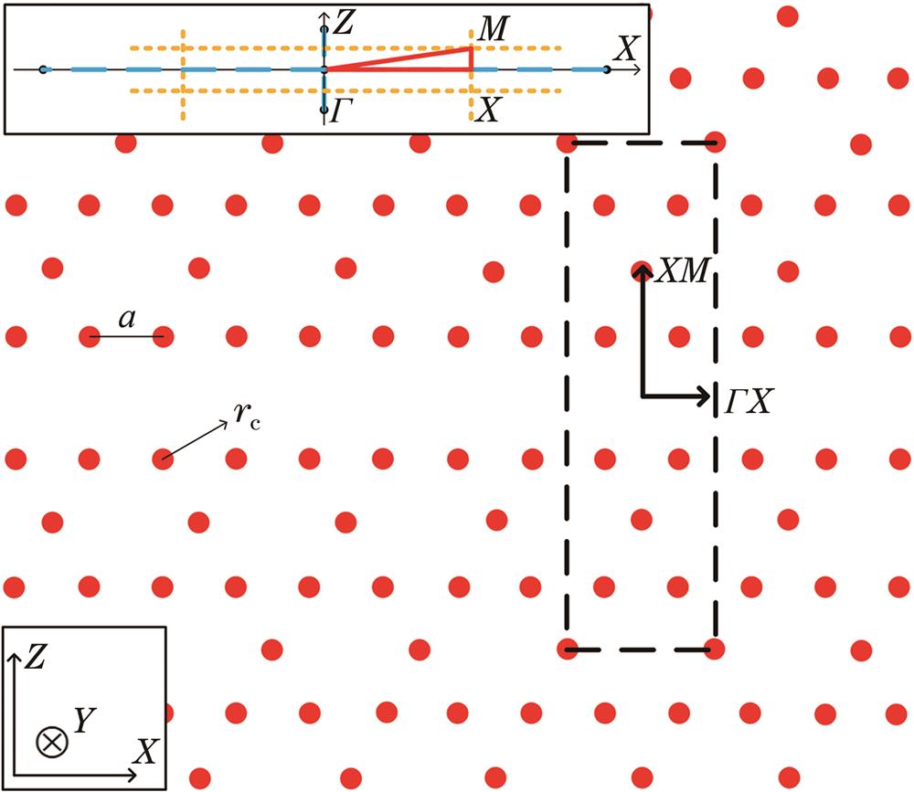
    Fig. 1. Line defect in Kagome lattice, black dot frame is the supercell schematic and inset in the upper left is the Brillouin region
    Simulation results of the line defect in Kagome lattice. (a) TM energy band structure; (b) transmission spectrum
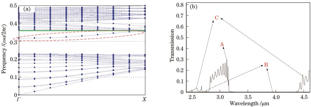
    Fig. 2. Simulation results of the line defect in Kagome lattice. (a) TM energy band structure; (b) transmission spectrum
    Steady-state field distribution of beams of different wavelengths and variation of light intensity value with time. (a) λ=3.124 μm; (b) λ=3.75 μm; (c) λ=4.597 μm
    Fig. 3. Steady-state field distribution of beams of different wavelengths and variation of light intensity value with time. (a) λ=3.124 μm; (b) λ=3.75 μm; (c) λ=4.597 μm
    Waveguide based on Kagome lattice. (a) Waveguide structure parameters; (b) relationship between the first band gap width and rc
    Fig. 4. Waveguide based on Kagome lattice. (a) Waveguide structure parameters; (b) relationship between the first band gap width and rc
    Relationship between transverse wave vector frequencies of waveguide mode and rd
    Fig. 5. Relationship between transverse wave vector frequencies of waveguide mode and rd
    Newly designed Kagome lattice waveguide.(a) New defect structure; (b) relationship between its defect mode frequency and rd
    Fig. 6. Newly designed Kagome lattice waveguide.(a) New defect structure; (b) relationship between its defect mode frequency and rd
    TM energy band structure of each node in Fig. 6(b). (a) rd=0.06a; (b) rd=0.09a; (c) rd=0.14a; (d) rd=0.18a
    Fig. 7. TM energy band structure of each node in Fig. 6(b). (a) rd=0.06a; (b) rd=0.09a; (c) rd=0.14a; (d) rd=0.18a
    When rd=0.1a, relationship between defect mode frequency and l
    Fig. 8. When rd=0.1a, relationship between defect mode frequency and l
    TM band structures of the line defect. (a) Before the movement; (b) after the movement (l=0.5a)
    Fig. 9. TM band structures of the line defect. (a) Before the movement; (b) after the movement (l=0.5a)
    Relationship between defect mode frequency and r1
    Fig. 10. Relationship between defect mode frequency and r1
    Optimized Kagome lattice. (a) Optimized Kagome line defect structure; (b) transmission spectrum
    Fig. 11. Optimized Kagome lattice. (a) Optimized Kagome line defect structure; (b) transmission spectrum
    Yanhong Yao, Lü Qieni, Xiaopeng Chen, Mingdi Zhang, Miaomiao Zhang. A Few-Mode Waveguide Structure Based on Kagome Lattice[J]. Laser & Optoelectronics Progress, 2022, 59(3): 0316001
    Download Citation