• Photonics Research
  • Vol. 10, Issue 1, 8 (2022)
Gengxin Chen1, Ziliang Ruan1, Zong Wang2, Pucheng Huang2, Changjian Guo2、3, Daoxin Dai1, Kaixuan Chen2、3、4, and Liu Liu1、*
Author Affiliations
  • 1State Key Laboratory for Modern Optical Instrumentation, College of Optical Science and Engineering, International Research Center for Advanced Photonics, Zhejiang University, Hangzhou 310058, China
  • 2Guangdong Provincial Key Laboratory of Optical Information Materials and Technology, South China Academy of Advanced Optoelectronics, South China Normal University, Higher-Education Mega-Center, Guangzhou 510006, China
  • 3National Center for International Research on Green Optoelectronics, South China Normal University, Guangzhou 510006, China
  • 4e-mail: chenkaixuan@m.scnu.edu.cn
  • show less
    DOI: 10.1364/PRJ.438816 Cite this Article Set citation alerts
    Gengxin Chen, Ziliang Ruan, Zong Wang, Pucheng Huang, Changjian Guo, Daoxin Dai, Kaixuan Chen, Liu Liu. Four-channel CWDM device on a thin-film lithium niobate platform using an angled multimode interferometer structure[J]. Photonics Research, 2022, 10(1): 8 Copy Citation Text show less
    (a) Schematic diagram of the four-channel CWDM on TFLN based on an angled MMI structure. (b) Calculated wavelength dependence of the neff curve for the first five TE modes at WMMI=17.54 μm. (c) Calculated neff curve of the first five TE modes at different WMMI at a wavelength of 1300 nm. (d) Simulated light propagation in the proposed angled MMI structure.
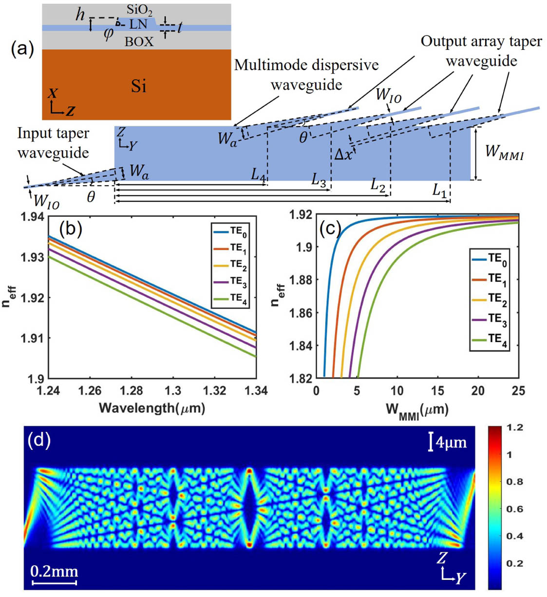
    Fig. 1. (a) Schematic diagram of the four-channel CWDM on TFLN based on an angled MMI structure. (b) Calculated wavelength dependence of the neff curve for the first five TE modes at WMMI=17.54  μm. (c) Calculated neff curve of the first five TE modes at different WMMI at a wavelength of 1300 nm. (d) Simulated light propagation in the proposed angled MMI structure.
    Simulated spectral responses of the proposed CWDM device with different tilted angles: (a) θ=0.17 rad, (b) θ=0.15 rad, and (c) θ=0.23 rad. The output waveguide spacing here is Δx=0.88 μm.
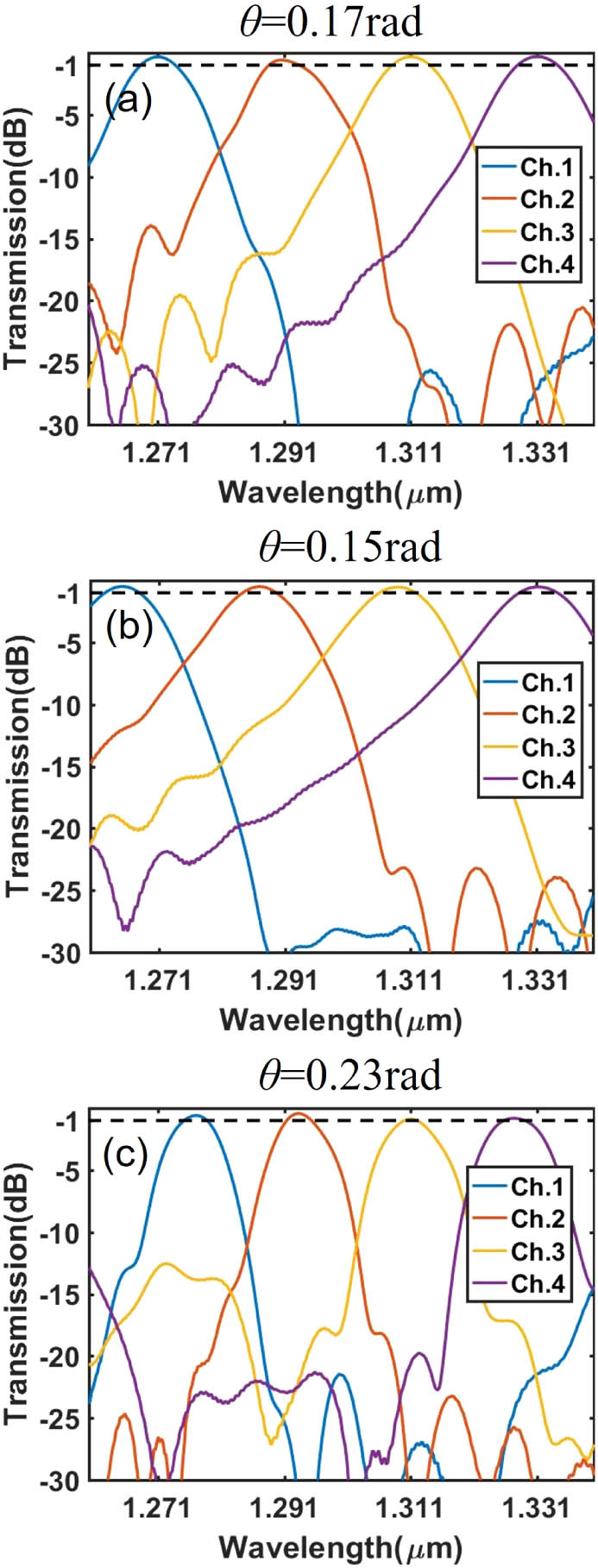
    Fig. 2. Simulated spectral responses of the proposed CWDM device with different tilted angles: (a) θ=0.17  rad, (b) θ=0.15  rad, and (c) θ=0.23  rad. The output waveguide spacing here is Δx=0.88  μm.
    Simulated spectral responses of the proposed CWDM device for (a) θ=0.15 rad, Δx=0.1 μm and (b) θ=0.23 rad, Δx=2.79 μm.
    Fig. 3. Simulated spectral responses of the proposed CWDM device for (a) θ=0.15  rad, Δx=0.1  μm and (b) θ=0.23  rad, Δx=2.79  μm.
    Simulated fabrication tolerance of the proposed CWDM device with changes (a) in L1 of ΔL1 from −1 to +1 μm, (b) in WMMI of ΔWMMI from −0.04 to +0.04 μm, (c) only in input waveguide width Wa of ΔWa from −2.4 to +2.4 μm, (d) in both input and output waveguide widths Wa of ΔWa from −4 to +4 μm, (e) in t of Δt from −20 to +20 nm, and (f) in h of Δh from −20 to +20 nm for channel #1. Except for the one studied, the rest of the structural parameters are unchanged as shown in Table 1.
    Fig. 4. Simulated fabrication tolerance of the proposed CWDM device with changes (a) in L1 of ΔL1 from 1 to +1  μm, (b) in WMMI of ΔWMMI from 0.04 to +0.04  μm, (c) only in input waveguide width Wa of ΔWa from 2.4 to +2.4  μm, (d) in both input and output waveguide widths Wa of ΔWa from 4 to +4  μm, (e) in t of Δt from 20 to +20  nm, and (f) in h of Δh from 20 to +20  nm for channel #1. Except for the one studied, the rest of the structural parameters are unchanged as shown in Table 1.
    (a) Microscope image of a fabricated device. Scanning electron microscope images of (b) input coupling grating, (c) input waveguide, (d) output waveguides, and (e) output coupling gratings.
    Fig. 5. (a) Microscope image of a fabricated device. Scanning electron microscope images of (b) input coupling grating, (c) input waveguide, (d) output waveguides, and (e) output coupling gratings.
    (a) Schematic of the measurement setup. (b) Measured spectral response of the fabricated CWDM device. (c) Measured peak wavelength positions (red dots), linear fit (red dotted line), and simulated peak wavelength positions (blue dots) for channel #1 with variations in WMMI.
    Fig. 6. (a) Schematic of the measurement setup. (b) Measured spectral response of the fabricated CWDM device. (c) Measured peak wavelength positions (red dots), linear fit (red dotted line), and simulated peak wavelength positions (blue dots) for channel #1 with variations in WMMI.
    WMMI=17.54  μm, Wa=5.54  μm, θ=0.17  rad, Δx=0.88  μm, i=1,2,3,4
    Channel #1234
    λi [nm]1271129113111331
    Li [μm]2054201719801943
    Table 1. Optimized Structural Parameters for the Four-Channel CWDM Device on TFLN
    WMMI=17.54  μm, Wa=5.54  μm, i=1,2,3,4
    Channel # 1234
    θ=0.15  radλi [nm]1265128713091331
    Δx=0.88  μmLi [μm]2064202319821941
    θ=0.23  radλi [nm]1277129213071322
    Δx=0.88  μmLi [μm]2041201319851957
    Table 2. Structural Parameters of the Four-Channel CWDM Device on TFLN for Figs. 2(b) and 2(c)
    WMMI=17.54  μm, Wa=5.54  μm, i=1,2,3,4
    Channel #1234
    θ=0.15  radλi [nm]1271129113111331
    Δx=0.10  μmLi [μm]2053201519771939
    θ=0.23  radλi [nm]1271129113111331
    Δx=2.79  μmLi [μm]2053201719811945
    Table 3. Structural Parameters of the Four-Channel CWDM Device on TFLN for Figs. 3(a) and 3(b)
    DeviceFootprint (mm2)Channel Amount/Spacing (nm)Insertion Loss (dB)XTcentera (dB)BW3dB
    Si [19] PCG0.25 × 0.164/20.22.223.3NMb
    Si [20] CMZI0.3 × 0.14/2012019
    Si [22] MMI0.012 × 1.214/2122012
    Si [25] MWGc0.6 × 0.044/2012015d
    SiN [26] CMZI1 × 0.64/201.815–2412d
    USRN [27] CVGe0.0006 × 8f8/201257.7
    SiN [23] MMI0.02 × 1.74/191.516–2711
    SiN [21] MWG0.23 × 1.954/20<1.081810d
    This work0.02 × 2.14/20<0.721812.1
    Table 4. Performance Comparison of Different Types of CWDM Devices
    Gengxin Chen, Ziliang Ruan, Zong Wang, Pucheng Huang, Changjian Guo, Daoxin Dai, Kaixuan Chen, Liu Liu. Four-channel CWDM device on a thin-film lithium niobate platform using an angled multimode interferometer structure[J]. Photonics Research, 2022, 10(1): 8
    Download Citation