
Ke Sun, Shengzhi Sun, Jianrong Qiu. Research Progress on Ultrashort Pulsed Laser Welding of Non-Metallic Materials[J]. Laser & Optoelectronics Progress, 2020, 57(11): 111422
- Laser & Optoelectronics Progress
- Vol. 57, Issue 11, 111422 (2020)
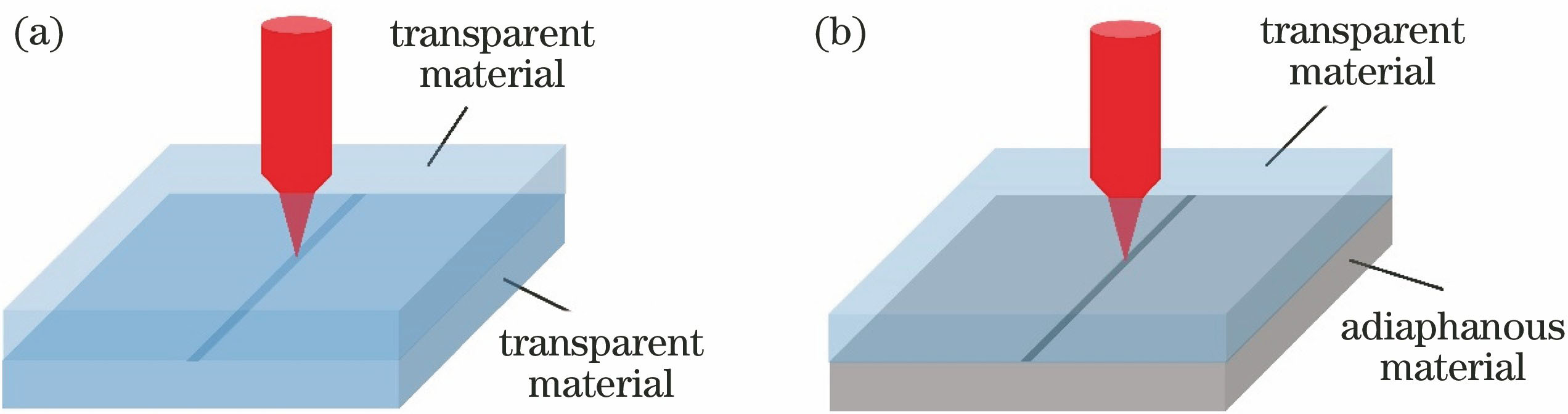
Fig. 1. Schematic diagram of ultrashort pulsed laser welding. (a) Welding of fully transparent materials; (b) welding of partial transparent materials
![Microscopic side view images for different focusing depths[23]. (a) Focus point locates at the interface; (b) focus point locates under the interface](/richHtml/lop/2020/57/11/111422/img_2.jpg)
Fig. 2. Microscopic side view images for different focusing depths[23]. (a) Focus point locates at the interface; (b) focus point locates under the interface
Fig. 3. Microscopic side view images for different focusing depths[26]. (a) Samples welded by femtosecond laser Bessel beam with different focus positions; (b) samples welded by femtosecond laser Gaussian beam with different focus positions
Fig. 4. Micro-morphology and macro-performance testing of weld[32]. (a) SEM image of cross section of YSZ ceramics near laser-affected zone; (b) SEM image of cross section of alumina oxide ceramics near laser-affected zone; (c) vacuum pressure versus time (leak-rate measurements); (d) shear test results
Fig. 5. Breaking stress of joint of monocrystalline silicon and glass[34]
Fig. 6. Microscopic image of cleaved PMMA surface after welding of PMMA substrates[38]
Fig. 7. Cross sections of weld[40]. (a) Cross section of weld at laser power of 1700 mW; (b) top view of weld at laser power of 1000 mW
Fig. 8. Optical micrograph of ceramic cavity sealed with glass substrate[31]
Fig. 9. Schematic of sealed microfluidic devices formed by femtosecond laser welding and top view of sealed microfluidic device[43]
Fig. 10. Schematics of processes employed in microfluidic device fabrication[44]. (a) Fabrication channel; (b) cutting inlets; (c) filter screen of 3D fabrication; (d) laser welding
Fig. 11. Photos of microfluidic samples fabricated by femtosecond laser welding[44]
Fig. 12. Picture of underwater welding parts[42]

Set citation alerts for the article
Please enter your email address
© Copyright 2018-2021 | Chinese Laser Press. All Rights Reserved 沪ICP备15018463号-20