
Tian Sun, Weiliang Ma, Donghua Liu, Xiaozhi Bao, Babar Shabbir, Jian Yuan, Shaojuan Li, Dacheng Wei, Qiaoliang Bao. Graphene plasmonic nanoresonators/graphene heterostructures for efficient room-temperature infrared photodetection[J]. Journal of Semiconductors, 2020, 41(7): 072907
- Journal of Semiconductors
- Vol. 41, Issue 7, 072907 (2020)
Abstract
1. Introduction
High-performance mid-infrared (mid-IR) photodetectors are widely used in security and biomedical areas[
Controlling light at the sub-wavelength scale plays a pivotal role in a wide variety of areas ranging from physics and photonics to biology[
Here, we demonstrated graphene-based mid-IR photodetector enhanced by the plasmonic effect from another layer of as-grown GNRs array. The array of GNRs was prepared by quasi-equilibrium plasma-enhanced chemical vapor deposition method, which is ultra-clean and size-controllable. We imaged the mid-IR “hot spot” in arrays by investigating the localized modes of graphene plasmon in individual GNRs using scattering-type scanning near-field optical microscopy (s-SNOM) in real space. Our study will shed new light on the efficient mid-IR light-harvesting device.
2. Experiment
2.1. Growth of GNRs and Fabrication of the device
GNRs were prepared by qe-PECVD. The details can refer to the Ref. [38]. We control the size and density of GNRs by the methane gas flow, the time and temperature of growth. The GNRs were directly obtained on the SiO2/Si substrate. The GNRs/graphene heterostructure was fabricated by placing the PMMA-supported CVD graphene on top of the GNRs covered by thin layer h-BN. The devices were patterned by using the standard UV lithography. The electrodes are deposited with electron-beam evaporation.
2.2. s-SNOM set up
The mid-IR imaging described in the main text was performed using a commercial s-SNOM (Neaspec Company. Bunsenstr. 5 D-82152 Martinsried [Munich] Germany www.neaspec.com) equipped with a CO2 laser (Access Laser Company. 917 134th St SW, Suite A1 Everett, WA 98204. www.accesslaser.com). The laser used here covers a wavelength range of 10.8–11.3 μm. The incident IR light is focused on the Pt-coated high-frequency oscillating AFM tip, and the tapping frequency and amplitude are approximately 270 kHz and 50 nm, respectively. The backscattered light is recorded via pseudo heterodyne detection, and the detected signal is then demodulated at the 3rd harmonic of the tip vibration frequency.
2.3. Simulation of graphene plasmons in GNRs
The numerical calculations were done in our work using the finite boundary elements method (commercial Comsol software). The graphene was defined as a two-dimensional conducting layer with the conductivity. The conductivity of graphene was modeled as random-phase approximation[
The α, γ and t present the frequency, decay rate and temperature. By slightly tuning the value of decay rate, we can obtain the well agreement with the experiments.
3. Result and discussion
3.1. Graphene nano-disk characterizations
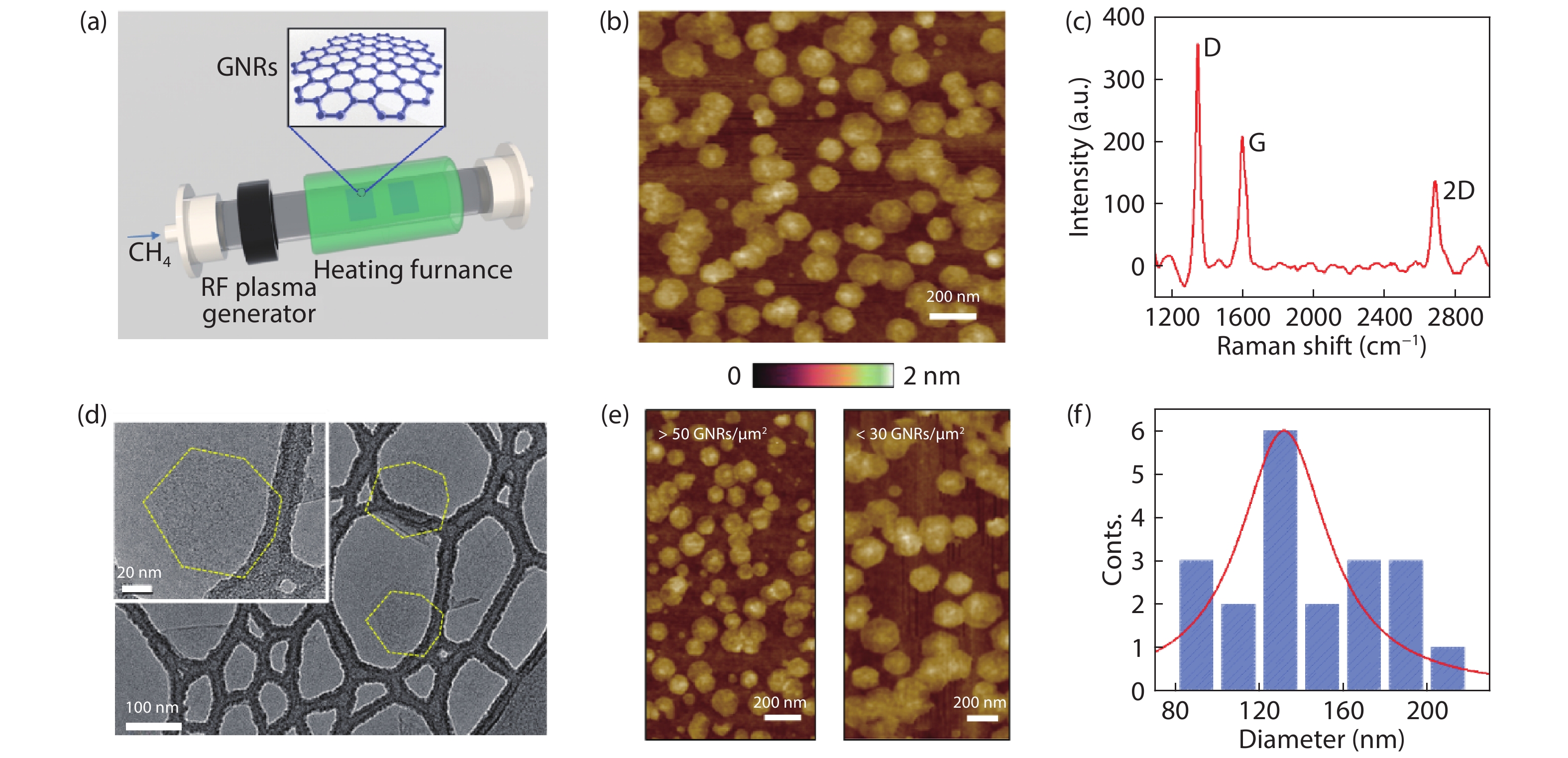
The graphene nano-disks were grown by the quasi-equilibrium plasma-enhanced chemical vapor deposition (qe-PECVD) system, which is illustrated in Fig. 1(a). The radio frequency plasma generator introduces the methane plasma into the quartz tube of the tubular furnace. The size and distribution of graphene nano-disks are highly controllable by tuning the factor during the growth process. The details of growth can be referred to as the former work[
![]()
Figure 1.(Color online) Characterization results of GNRs: AFM, HRTEM image and Raman spectrum, density and size distribution. (a) Representation of growth process of GNRs. The GNRs were obtained on the SiO2/Si substrate by qe-PECVD. Upper image: Schematic illustration of the GNRs. (b) Atomic force microscope (AFM) image of GNRs. (c) The Raman spectrum shows the characteristic band (D, G, 2D) of GNRs. (d) A HRTEM image of GNRs. Scale bar: 100 nm. An enlarged HRTEM image. Scale bar: 20 nm. (e) The controlled density of GNRs, the AFM image indicate two different densities. Scale bar: 200 nm. (f) Statistical distribution of the diameter of GNRs with Gaussian fits overlaid.
3.2. IR “hot spot” in GNRs
Over the past decade, graphene plasmon has received considerable attention for a wide range of applications especially in the technically important mid-IR to THz frequency ranges, such as in molecular sensors, terahertz detectors, and highly surface-enhanced Raman spectroscopy because of its ultrahigh confinement, facile processability and tunability via electric fields[
Fig. 2(a) schematically illustrates the excitation of graphene plasmon in GNRs under s-SNOM. IR light (10.8–11.3 μm) is focused onto the Pt-coated high-frequency oscillating tip of an AFM. The tip also works as an optical antenna which launches a wave vector stronger than that of the incident light to match the excitation conditions of the graphene plasmon[
![]()
Figure 2.(Color online) Schematics and mid-IR “hot-spot” of GNRs imaging with s-SNOM. (a) Simplified schematics of s-SNOM measurements: The Pt-coated tip is illuminated by mid-IR light and interacts with GNRs to launch and detect a graphene plasmon and their localized F-P modes in GNRs. (b) Near-field amplitude image of GNRs at
Fig. 2(b) shows the characteristic near-field amplitude s(ω) of GNRs at mid-IR. Several significant near-field features of GNRs can be observed: a bright spot in the center of small GNRs and a bright ring but a dark center in bigger GNRs. The different features indicate the various circular breathing modes in different GNRs[
For unravel the accurate relationship between the near-field distribution and diameter of GNRs as well as excitation wavelength. We simulated the excitation of surface plasmon in GNRs, and the results are depicted in Figs. 2(e) and 2(f). Here we present the simulated near-field distribution around the GNRs at fixed dipole positions, the dipole is located 25 nm above the center of single GNR. For the fixed excitation wavelength (as shown in Fig. 2(e)), the wavelength of graphene plasmon is also fixed. Here we can see the clear positive and negative near-field contrast. The diameter of GNRs influences the near-field amplitude at the center and affects the graphene plasmon interference in the F-P cavity, which is GNR here. The longer excitation wavelength leads to less period of near-field distribution in GNRs with a fixed diameter (as shown in Fig. 2(f)), which suggests a linear relationship between λsp and λ0. The simulated results generally agree with our experimental observations (as shown in Figs. 2(b) and 2(d)) and also are consistent with previous work[
3.3. Room temperature mid-IR photodetector based on GNRs/graphene heterostructure
Considering the potential for enhanced light-matter interaction of GNRs, we combine the GNRs with pure monolayer graphene to fabricate GNRs/graphene vertical heterostructure for mid-IR photodetectors. Fig. 3(a) shows the optical image of the individual device in which the interdigitated antenna electrodes can efficiently help to capture more mid-IR light. As shown in Fig. 3(b), the schematic illustration of mid-IR photodetector based on GNRs/graphene heterostructure device are presented. The device structure comprises Ti/Au (10 nm/100 nm) electrodes, GNRs, hexagonal boron nitride (h-BN), and monolayer graphene. A thin layer of h-BN (thickness: 2 nm) is sandwiched between graphene and GNRs as a dielectric layer and plays an important role to prevent non-equilibrium carriers from transferring between materials.
![]()
Figure 3.(Color online) Room temperature mid-IR photodetector based on GNRs/graphene heterostructure. (a) Optical image of heterostructure mid-IR photodetector with efficient interdigitated antenna electrodes, Scale bar: 50
Fig. 3(c) plots the characteristic curves of photocurrent (Iph= Ilight – Idark) versus bias voltage (VSD) for pure graphene photodetector (black), GNRs/graphene heterostructure photodetector with different GNRs density. All the measurements were performed at room temperature. When IR light focused to a beam spot with a diameter of 1 cm is irradiated to the surface of the heterostructure, the electron-hole pairs are generated immediately in graphene film and collected by electrodes driven by an external electrical field. It is notable that the photocurrent in GNRs/graphene hybrid devices is much larger than that in pure graphene photodetector. Interestingly, the larger the density of GNRs in the heterostructure, the higher the photocurrent in the device. We conclude that graphene in this heterostructure absorbs more mid-IR light than pure graphene and more GNRs could help to localize more IR photons, thus increasing the absorption capacity in graphene. The inset of Fig. 3(c) shows the representative AFM image of GNRs with different densities. Fig. 3(d) shows the photocurrent changes periodically when switching on and off the incident laser at 10.6 μm and the photoresponse time is relatively long considering general thermal effect in IR radiation. For GNRs/graphene heterostructure photodetector with large GNRs density, the photocurrent as a function of VSD at different incident powers and time-dependent photocurrent response are shown in Figs. 3(e) and 3(f). The photocurrent increases almost linearly while VSD increases. It is worth pointing out that the photo response remains identical after several tens of switching cycles. The key figure-of-merit parameters of the device, responsivity (R), is given by
4. Conclusion
Our work investigated the plasmonic properties of as-grown graphene nano-disk GNRs and explored the mid-IR photodetection properties of GNRs/graphene heterostructure. By using IR nano-imaging techniques, we found that near-field confinement in GNRs shows a strong dependence on diameter and excitation wavelength. The performance of graphene mid-IR photodetector can be enhanced by incorporating GNRs to enhance the light absorption, and it can be further modulated by controlling the density of GNRs. Notably, our work envisions the huge potential of as-grown nanostructured graphene for photonic applications, which cover a broad range in the technologically important IR bands.
Acknowledgement
We acknowledge support from the National Key Research & Development Program (No. 2016YFA0201902, 2018YFA0703200), Shenzhen Nanshan District Pilotage Team Program (LHTD20170006), National Natural Science Foundation of China (61974099 and 61604102, 51773041, 61890940), Shanghai Committee of Science and Technology in China (18ZR1404900), Natural Science Research Project for Anhui Universities (Grant No. KJ2019A0596), Youth Project of Provincial Natural Science Foundation of Anhui (Grant No. 2008085QF319) and Australian Research Council (ARC, FT150100450 and IH150100006).
References
[1] H Schneider, F Fuchs, B Dischler et al. Intersubband absorption and infrared photodetection at 3.5 and 4.2
[2] A Naumann, M Navarro-González, S Peddireddi et al. Fourier transform infrared microscopy and imaging: Detection of fungi in wood. Fungal Genet Biol, 42, 829(2005).
[3] Y F Lao, A G Unil Perera, L H Li et al. Tunable hot-carrier photodetection beyond the bandgap spectral limit. Nat Photonics, 8, 412(2014).
[4] X L Chen, X B Lu, B C Deng et al. Widely tunable black phosphorus mid-infrared photodetector. Nat Commun, 8, 1672(2017).
[5] M Freitag, T Low, W J Zhu et al. Photocurrent in graphene harnessed by tunable intrinsic plasmons. Nat Commun, 4, 1951(2013).
[6] M Amani, E Regan, J Bullock et al. Mid-wave infrared photoconductors based on black phosphorus-arsenic alloys. ACS Nano, 11, 11724(2017).
[7] Y M Lin, C Dimitrakopoulos, K A Jenkins et al. 100-GHz transistors from wafer-scale epitaxial graphene. Science, 327, 662(2010).
[8] Q L Bao, K P Loh. Graphene photonics, plasmonics, and broadband optoelectronic devices. ACS Nano, 6, 3677(2012).
[9] L Vicarelli, M S Vitiello, D Coquillat et al. Graphene field-effect transistors as room-temperature terahertz detectors. Nat Mater, 11, 865(2012).
[10] B Sensale-Rodriguez, R S Yan, M M Kelly et al. Broadband graphene terahertz modulators enabled by intraband transitions. Nat Commun, 3, 780(2012).
[11] T Mueller, F N Xia, P Avouris. Graphene photodetectors for high-speed optical communications. Nat Photonics, 4, 297(2010).
[12] O Lopez-Sanchez, D Lembke, M Kayci et al. Ultrasensitive photodetectors based on monolayer MoS2. Nat Nanotechnol, 8, 497(2013).
[13] X D Wang, P Wang, J L Wang et al. Ultrasensitive and broadband MoS2 photodetector driven by ferroelectrics. Adv Mater, 27, 6575(2015).
[14] M S Long, P Wang, H H Fang et al. Progress, challenges, and opportunities for 2D material based photodetectors. Adv Funct Mater, 29, 1803807(2019).
[15] G Rao, M Freitag, H Y Chiu et al. Raman and photocurrent imaging of electrical stress-induced p–n junctions in graphene. ACS Nano, 5, 5848(2011).
[16] M Freitag, T Low, F N Xia et al. Photoconductivity of biased graphene. Nat Photonics, 7, 53(2013).
[17] M Buscema, J O Island, D J Groenendijk et al. Photocurrent generation with two-dimensional van der Waals semiconductors. Chem Soc Rev, 44, 3691(2015).
[18] X Zhou, X Z Hu, J Yu et al. 2D layered material-based van der Waals heterostructures for optoelectronics. Adv Funct Mater, 28, 1706587(2018).
[19] N J Huo, G Konstantatos. Recent progress and future prospects of 2D-based photodetectors. Adv Mater, 30, 1801164(2018).
[20] M W Knight, H Sobhani, P Nordlander et al. Photodetection with active optical antennas. Science, 332, 702(2011).
[21] Z Y Fang, Z Liu, Y M Wang et al. Graphene-antenna sandwich photodetector. Nano Lett, 12, 3808(2012).
[22] L Ju, B S Geng, J Horng et al. Graphene plasmonics for tunable terahertz metamaterials. Nat Nanotechnol, 6, 630(2011).
[23] H A Atwater, A Polman. Plasmonics for improved photovoltaic devices. Nat Mater, 9, 205(2010).
[24] J N Anker, W P Hall, O Lyandres et al. Biosensing with plasmonic nanosensors. Nat Mater, 7, 442(2008).
[25] R Hillenbrand, T Taubner, F Keilmann. Phonon-enhanced light–matter interaction at the nanometre scale. Nature, 418, 159(2002).
[26] A Boltasseva, H A Atwater. Low-loss plasmonic metamaterials. Science, 331, 290(2011).
[27]
[28] J B Khurgin, A Boltasseva. Reflecting upon the losses in plasmonics and metamaterials. MRS Bull, 37, 768(2012).
[29] J B Khurgin, G Sun. In search of the elusive lossless metal. Appl Phys Lett, 96, 181102(2010).
[30] J N Chen, M Badioli, P Alonso-González et al. Optical nano-imaging of gate-tunable graphene plasmons. Nature, 487, 77(2012).
[31] Z Fei, A S Rodin, G O Andreev et al. Gate-tuning of graphene plasmons revealed by infrared nano-imaging. Nature, 487, 82(2012).
[32] G X Ni, d A S McLeod, Z Sun et al. Fundamental limits to graphene plasmonics. Nature, 557, 530(2018).
[33] Z Y Fang, Y M Wang, A E Schlather et al. Active tunable absorption enhancement with graphene nanodisk arrays. Nano Lett, 14, 299(2014).
[34] H G Yan, T Low, W J Zhu et al. Damping pathways of mid-infrared plasmons in graphene nanostructures. Nat Photonics, 7, 394(2013).
[35] A Y Nikitin, P Alonso-González, S Vélez et al. Real-space mapping of tailored sheet and edge plasmons in graphene nanoresonators. Nat Photonics, 10, 239(2016).
[36] X X Yang, F Zhai, H Hu et al. Far-field spectroscopy and near-field optical imaging of coupled plasmon-phonon polaritons in 2D van der waals heterostructures. Adv Mater, 28, 2931(2016).
[37] Q Y Xu, T Ma, M Danesh et al. Effects of edge on graphene plasmons as revealed by infrared nanoimaging. Light: Sci Appl, 6, e16204(2017).
[38] D H Liu, X S Chen, Y B Hu et al. Raman enhancement on ultra-clean graphene quantum dots produced by quasi-equilibrium plasma-enhanced chemical vapor deposition. Nat Commun, 9, 193(2018).
[39] X Z Chen, D B Hu, R Mescall et al. Modern scattering-type scanning near-field optical microscopy for advanced material research. Adv Mater, 31, 1804774(2019).

Set citation alerts for the article
Please enter your email address
© Copyright 2018-2021 | Chinese Laser Press. All Rights Reserved 沪ICP备15018463号-20