• Laser & Optoelectronics Progress
  • Vol. 58, Issue 23, 2316006 (2021)
Yongzheng Hu*
Author Affiliations
  • Department of Foundation, China Fire and Rescue Institute, Beijing 102202, China
  • show less
    DOI: 10.3788/LOP202158.2316006 Cite this Article Set citation alerts
    Yongzheng Hu. Graphene Growth at the Interface of Sapphire Substrate and Nickel Layer[J]. Laser & Optoelectronics Progress, 2021, 58(23): 2316006 Copy Citation Text show less
    References

    [1] Raypah M E, Dheepan M K, Devarajan M et al. Investigation on thermal characterization of low power SMD LED mounted on different substrate packages[J]. Applied Thermal Engineering, 101, 19-29(2016).

    [2] Cai M, Yang D G, Mo Y Z et al. Determining the thermal stress limit of LED lamps using highly accelerated decay testing[J]. Applied Thermal Engineering, 102, 1451-1461(2016).

    [3] Krames M R, Shchekin O B, Mueller-Mach R et al. Status and future of high-power light-emitting diodes for solid-state lighting[J]. Journal of Display Technology, 3, 160-175(2007).

    [4] Kim H, Kim K K, Choi K K et al. Design of high-efficiency GaN-based light emitting diodes with vertical injection geometry[J]. Applied Physics Letters, 91, 023510(2007).

    [5] Chu C F, Lai F I, Chu J T et al. Study of GaN light-emitting diodes fabricated by laser lift-off technique[J]. Journal of Applied Physics, 95, 3916-3922(2004).

    [6] Han N, Cuong T V, Han M et al. Improved heat dissipation in gallium nitride light-emitting diodes with embedded graphene oxide pattern[J]. Nature Communications, 4, 1452(2013).

    [7] Sun Y J, Yu T J, Chen Z Z et al. Properties of GaN-based light-emitting diode thin film chips fabricated by laser lift-off and transferred to Cu[J]. Semiconductor Science and Technology, 23, 125022(2008).

    [8] Wu Q Q, Guo Y N, Sundaram S et al. Exfoliation of AlN film using two-dimensional multilayer hexagonal BN for deep-ultraviolet light-emitting diodes[J]. Applied Physics Express, 12, 015505(2019).

    [9] Wang L C, Liu W, Zhang Y Y et al. Graphene-based transparent conductive electrodes for GaN-based light emitting diodes: challenges and countermeasures[J]. Nano Energy, 12, 419-436(2015).

    [10] Chang H L, Chen Z L, Li W J et al. Graphene-assisted quasi-van der Waals epitaxy of AlN film for ultraviolet light emitting diodes on nano-patterned sapphire substrate[J]. Applied Physics Letters, 114, 091107(2019).

    [11] Chen Z L, Zhang X, Dou Z P et al. High-brightness blue light-emitting diodes enabled by a directly grown graphene buffer layer[J]. Advanced Materials, 30, 1801608(2018).

    [12] Li J M, Liu Z Q, Wei T B et al. Development summary of semiconductor lighting in China[J]. Acta Optica Sinica, 41, 0116002(2021).

    [13] Liu Z Y, Wang P P, Jin Z L et al. Free-form lens design for LED fishing lamp with stable illumination[J]. Acta Optica Sinica, 41, 0522003(2021).

    [14] Li M, Piao Y, Deng L J. Spatial resolution of naked eye three-dimensional integral imaging display based on LED screen[J]. Laser & Optoelectronics Progress, 57, 061004(2020).

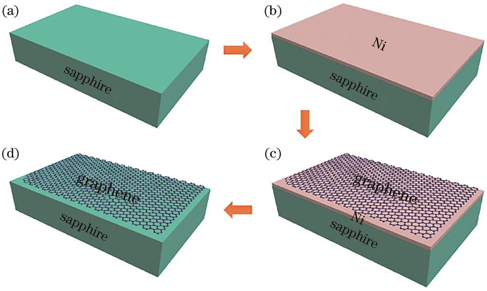
    [15] Kim J, Bayram C, Park H et al. Principle of direct van der Waals epitaxy of single-crystalline films on epitaxial graphene[J]. Nature Communications, 5, 4836(2014).

    [16] Koma A, Sunouchi K, Miyajima T. Fabrication and characterization of heterostructures with subnanometer thickness[J]. Microelectronic Engineering, 2, 129-136(1984).

    [17] Utama M I B, Zhang Q, Zhang J et al. Recent developments and future directions in the growth of nanostructures by van der Waals epitaxy[J]. Nanoscale, 5, 3570-3588(2013).

    [18] Chung K, Lee C H, Yi G C. Transferable GaN layers grown on ZnO-coated graphene layers for optoelectronic devices[J]. Science, 330, 655-657(2010).

    [19] Kim Y, Cruz S S, Lee K et al. Remote epitaxy through graphene enables two-dimensional material-based layer transfer[J]. Nature, 544, 340-343(2017).

    [20] Kim J, Park H, Hannon J B et al. Layer-resolved graphene transfer via engineered strain layers[J]. Science, 342, 833-836(2013).

    [21] Kobayashi Y, Kumakura K, Akasaka T et al. Layered boron nitride as a release layer for mechanical transfer of GaN-based devices[J]. Nature, 484, 223-227(2012).

    [22] Wang G, Zhao Y, Deng Y et al. Lattice selective growth of graphene on sapphire substrate[J]. The Journal of Physical Chemistry C, 119, 426-430(2015).

    [23] Su C Y, Lu A Y, Wu C Y et al. Direct formation of wafer scale graphene thin layers on insulating substrates by chemical vapor deposition[J]. Nano Letters, 11, 3612-3616(2011).

    Yongzheng Hu. Graphene Growth at the Interface of Sapphire Substrate and Nickel Layer[J]. Laser & Optoelectronics Progress, 2021, 58(23): 2316006
    Download Citation