
Yongzheng Hu. Graphene Growth at the Interface of Sapphire Substrate and Nickel Layer[J]. Laser & Optoelectronics Progress, 2021, 58(23): 2316006
- Laser & Optoelectronics Progress
- Vol. 58, Issue 23, 2316006 (2021)
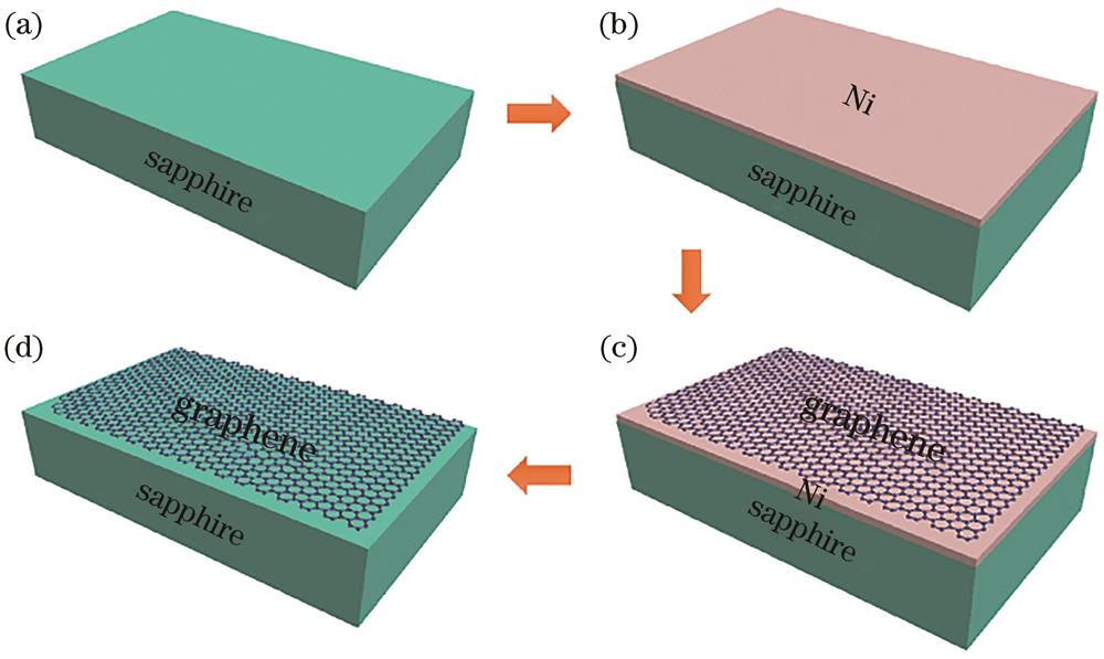
Fig. 1. Schematics of a method for growing few-layer graphene on sapphire substrate. (a) Sapphire substrate (c-plane) is prepared to synthesize graphene; (b) nickel is deposited on sapphire substrate by electron beam evaporation; (c) after growth, few-layered graphene forms on nickel's top surface of sapphire substrate; (d) after O2 plasma treatment on the surface and then etching away the nickel, few-layer graphene grown on the interface between nickel and c-plane sapphire can be found
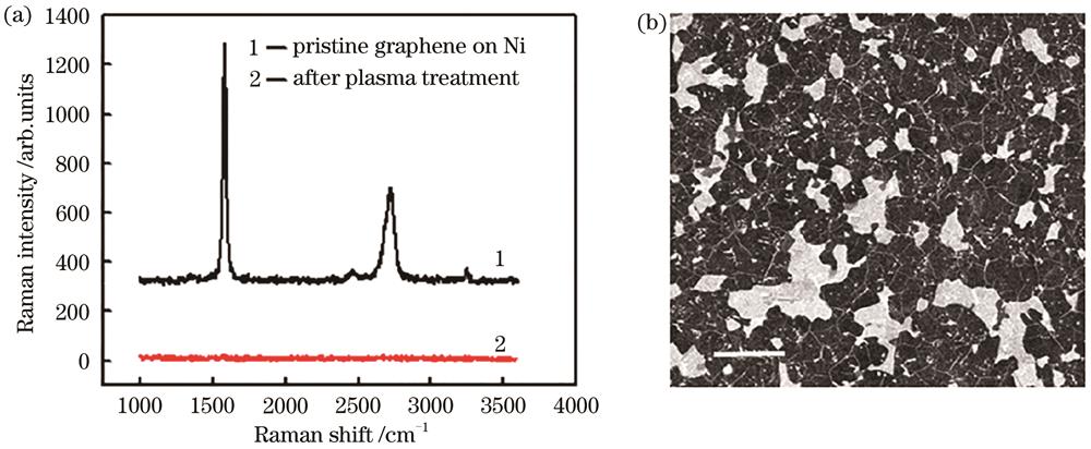
Fig. 2. Characterization of graphene on the surface of nickel film. (a) Raman spectra of graphene on the surface of nickel film before (curve 1) and after (curve 2) oxygen plasma treatment; (b) SEM image of graphene on the surface of nickel film,scale bar is 3.5 μm
Fig. 3. Characterization of graphene at the interface. (a) Raman spectra of graphene on the interface between nickel film and sapphire substrate after oxygen plasma treatment and etching away the nickel; (b) SEM image of graphene on the interface between nickel film and sapphire substrate,scale bar is 20 μm

Set citation alerts for the article
Please enter your email address
© Copyright 2018-2021 | Chinese Laser Press. All Rights Reserved 沪ICP备15018463号-20