
Bolin Zhou, Guohui Li, Jianhong Wu, Rong Wen, Huihui Pi, Yuying Hao, Yanxia Cui. Perovskite Photonic Crystal Laser with Low Threshold[J]. Laser & Optoelectronics Progress, 2022, 59(5): 0500005
- Laser & Optoelectronics Progress
- Vol. 59, Issue 5, 0500005 (2022)
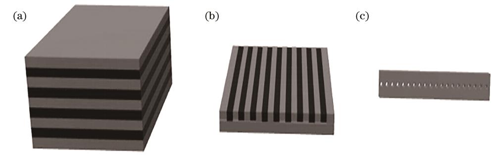
Fig. 1. Schematic of 1D photonic crystals. (a) Multilayer dielectric structure; (b) grating structure; (c) nanobeam structure
![DBR laser structure diagrams and photoluminescence line diagrams of different perovskite materials. (a) (b) Relationship between the photoluminescence intensity and pump energy of the DBR/CsPbBr3 QD/DBR structure laser photoluminescence intensity and pump energy of a DBR/CsPbBr3 QD/DBR laser[55]; (c) (d) DBR/MAPbBBr3 SC-TF/DBR structure laser, photoluminescence intensity and pump energy diagram[59]](/richHtml/lop/2022/59/5/0500005/img_2.jpg)
Fig. 2. DBR laser structure diagrams and photoluminescence line diagrams of different perovskite materials. (a) (b) Relationship between the photoluminescence intensity and pump energy of the DBR/CsPbBr3 QD/DBR structure laser photoluminescence intensity and pump energy of a DBR/CsPbBr3 QD/DBR laser[55]; (c) (d) DBR/MAPbBBr3 SC-TF/DBR structure laser, photoluminescence intensity and pump energy diagram[59]
Fig. 3. Perovskite DFB laser. (a) Schematic of DFB laser based on CsPbBrI2 perovskite; (b) functional relationship of output peak strength, FWHM and pump energy density [65]; (c) SEM image of of MAPbBr3 DFB laser (inset: high-resolution cross section, scale is 100 nm); (d) output intensity as a function of pump energy density[66]
Fig. 4. Nanobeam structure. (a) Schematic of the SiN nanobeam;(b) schematic of the CsPbBr3 perovskite nanocrystal coupled SiN nanobeam photonic crystal cavity; (c) fluorescence decay of perovskite nanocrystals under two different conditions [74]; (d) schematic of the CsPb (Br/I)3 perovskite nanocrystals coupled SiN nanobeam photonic crystal cavity; (e) cavity emission shows a nonlinear increase of the output intensity, while background emission shows a linear dependence on the pump intensity[27]
Fig. 5. (a) 2D photonic crystal structure diagram; (b) rectangular lattice air hole slab; (c) triangular lattice air hole slab
Fig. 6. Structure diagram and spectrum. (a) Schematic of the MAPbI3 Photonic crystal band-edge laser structure; (b) cross-section of the device[76]; (c) SEM image of the 2D Photonic crystal with dimensions of the triangular grating [inset (bottom): photograph of the sample under oblique while-light illumination. Inset (top): first Brillouin zone of the 2D photonic crystal with labelled points of high symmetry]; (d) lasing output characteristics along with the far field patterns slightly below and above threshold[26]
Fig. 7. (a) 3D PhC structure diagram; (b) schematic of colloidal crystal structure; (c) MAPbBr3 film is in the form of reverse opal, and the illustration is colloidal template; (d) spectra of inverted opal MAPbBr3 films at different incident energy densities[90]
|
Table 1. Thresholds and test conditions for photonics crystal laser with different materials

Set citation alerts for the article
Please enter your email address
© Copyright 2018-2021 | Chinese Laser Press. All Rights Reserved 沪ICP备15018463号-20