
Huaqing Qiu, Yong Liu, Xiansong Meng, Xiaowei Guan, Yunhong Ding, Hao Hu, "Bidirectional high sidelobe suppression silicon optical phased array," Photonics Res. 11, 659 (2023)
- Photonics Research
- Vol. 11, Issue 4, 659 (2023)
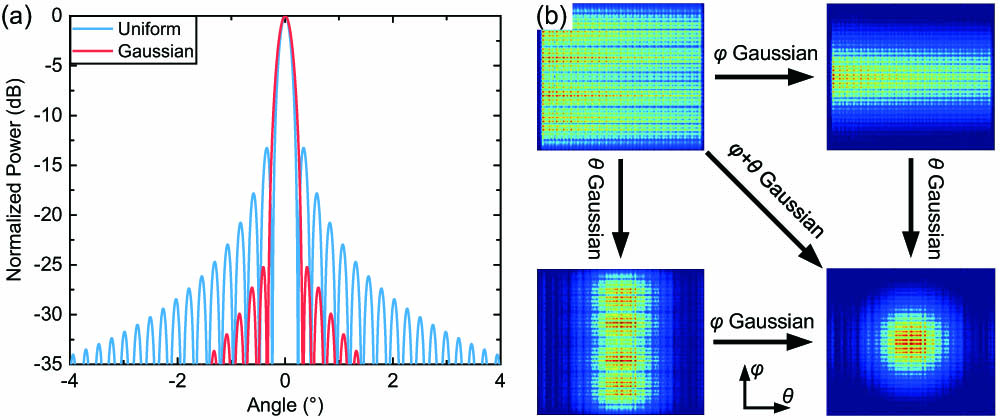
Fig. 1. (a) Simulation results for uniform power distribution and Gaussian power distribution. (b) Simulated near field of uniform power distribution and Gaussian power distribution for φ θ φ + θ

Fig. 2. (a) Schematic of the through-type cascaded coupler with Gaussian power distribution. (b) Required power, residual power, and coupling efficiency for the largest Gaussian center-to-edge ratio. (c) The largest SLSR is only 20 dB for the through-type cascaded coupler. (d) Schematic of the Y-branch-assisted cascaded coupler with Gaussian power distribution. (e) Required power, residual power, and coupling efficiency for the largest Gaussian center-to-edge ratio. (f) The largest SLSR can achieve 66 dB for the Y-branch-assisted cascaded coupler.
Fig. 3. (a) Designed 12 dB Gaussian power distribution on 120-channel OPA. (b) Far-field figure with SLSR of 25 dB. (c) Required power, residual power, and coupling efficiency for each channel. (d) Coupling length for each channel.
Fig. 4. (a) Apodized grating emitter with Gaussian power distribution in the near field. (b) Zoomed-in figure in (a).
Fig. 5. (a) Designed 12-dB Gaussian power distribution along 2-mm-long apodized grating emitter. (b) Corresponding SLSR in the far-field figure. (c) Simulated emitting efficiency per pitch and SiO 2
Fig. 6. (a) Schematic of proposed dual-Gaussian power distribution OPA. (b) Microscopy of proposed OPA. (c) SEM image of the apodized grating emitter with the largest SiO 2
Fig. 7. (a) Schematic of the measurement setup. (b) The 2.1 cm × 2.1 cm
Fig. 8. (a) Far-field figure before and after calibration. (b) Far-field figure in φ φ φ = − 2.4 ° θ
Fig. 9. (a) Peak-to-valley far-field intensity vibration when phase varies from 0 to 2 π
Fig. 10. (a) Far-field figure of the beam steered in φ φ φ φ
Fig. 11. (a) Far-field figure of the beam steered in θ θ θ φ θ
Fig. 12. (a) Schematic of cascaded couplers. (b) Simulated relationship between coupling efficiency and coupling length. (c) Experimental measurement results for designed 15 dB Gaussian power distribution along 64 channels.
Fig. 13. Number of channel limitations for through-type cascaded couplers. (a) The maximum number of channels is 420 for uniform power distribution. (b) Corresponding coupling lengths. (c) Power distribution, residual power before the n n
Fig. 14. Number of channel limitations for Y-splitter-assisted cascaded couplers. (a) The maximum number of channels can reach 1024 with 12 dB Gaussian power distribution. (b) Corresponding far-field pattern with SLSR of 25 dB. (c) Power distribution, residual power before the n
Fig. 15. (a) Periodic grating emitter with a fixed SiO 2 Λ = 0.7 μm θ 0 = 8.4 ° SiO 2 n eff SiO 2 SiO 2
Fig. 16. Principle of PWM technique.
Fig. 17. Gradient algorithm optimization process.
Fig. 18. (a) The far-field intensity changes when electric power increases from 0 to 7 mW, indicating power consumption of 2.7 mW / π φ
Fig. 19. (a) Measured PWM signal [30]. (b) Every three I/O ports share a common ground in the designed OPA. (c) Improved electric circuits of individual ground.
|
Table 1. Performance Comparison among State-of-the-Art Periodic 1D OPAs


Set citation alerts for the article
Please enter your email address

© Copyright 2018-2021 | Chinese Laser Press. All Rights Reserved 沪ICP备15018463号-20