
[in Chinese], [in Chinese], [in Chinese], [in Chinese]. Remote-mode microsphere nano-imaging: new boundaries for optical microscopes[J]. Opto-Electronic Advances, 2018, 1(1): 170001
- Opto-Electronic Advances
- Vol. 1, Issue 1, 170001 (2018)
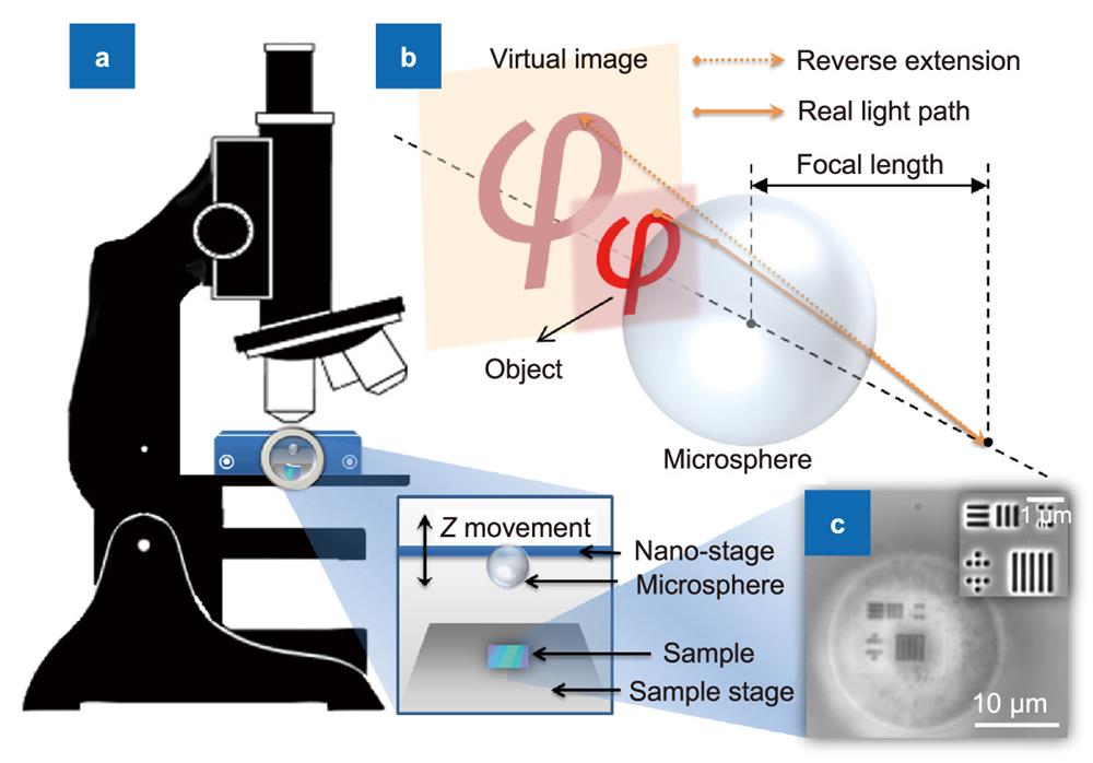
Fig. 1. (
a
) Schematic diagram of the remote mode optical microsphere setup. (
b
) Mechanism to illustrate the enlarged virtual image by the microsphere. (
c
) Optical image captured by this system (Sample: semiconductor testing sample; scale bar: 10 μm; imaged by a 20 μm silica microsphere compiled to an oil-immersion optical microscope with a 100× objective lens, NA=1.4). Inset: SEM image (scale bar: 1 μm).
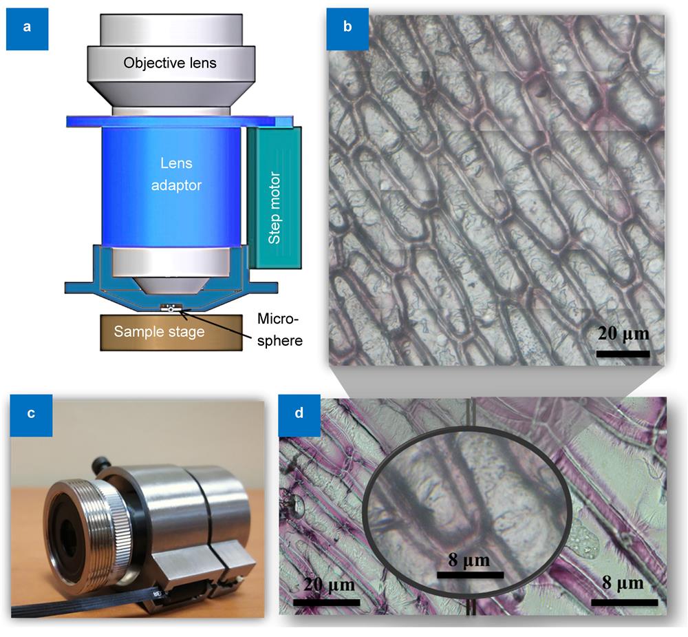
Fig. 2. (
a
) Schematic of the design of the universal lens adaptor for the microsphere (silica microsphere with 400 μm diameter attached on a 20× objective lens. Characterization was done in ambient air and distance between the onion cell and the microsphere is ~65 μm, with white light illumination). (
b
) Integrated image of onion cells (scale bar: 20 μm). (
c
) Optical image of the universal sample adaptor after integration. (
d
) Comparison of the optical images by three optical lenses: the 20× objective lens (left, scale bar: 20 μm); 20× objective lens with the microsphere (middle, which is our nanoscope design, scale bar: 8 μm); and 50× objective lens (right, scale bar: 8 μm).
Fig. 3. (
a
~
c
) Imaging of nano-dot pairs with nano-gap on a Si wafer. (
a
) SEM image of the samples, showing sizes of nano-gaps in between each pair of nano-dots. (
b
) Imaging of the samples by an oil-immersion microscope (neighboring nano-dots cannot be resolved clearly). (
c
) Neighboring separated nano-dots are resolved clearly by a microsphere with 20 μm diameter. The back dash line in (
c
) indicates the line cut (the intensity analysis is presented in supplementary materials). (
d
~
f
) Imaging of samples with complex features (the "nano-rose"). (
d
) Zoomed-in SEM image with size notations, it shows that the typical line width of the structure is ~140 nm, and separated by nano-grooves with a typical size ranging from 50~60 nm. (
e
) Imaging result by the oil-immersion optical microscope. (
f
) Image under the 27μm microsphere in scanning mode. The diameter of the microsphere is larger in order to contain the entire nano-rose in the central region. (Compared to the microsphere used for the imaging of nano-dots, the microsphere with a larger diameter is chosen to ensure the entire nano-rose pattern is in the central region of the microsphere. Inset: zoomed-in image under the microsphere). (
g
~
i
) Imaging of a magnetic head in a hard disc drive from the production line. (
g
) SEM image of the magnetic head, with a nano-gap of 77 nm. (
h
) Imaging by a conventional oil-immersion microscope. (
i
) Imaging by the microsphere nanoscope in non-contact mode. The three columns represent images obtained by SEM, oil-immersion optical microscope (100×, NA 1.4), and microsphere nanoscope, respectively.

Set citation alerts for the article
Please enter your email address
© Copyright 2018-2021 | Chinese Laser Press. All Rights Reserved 沪ICP备15018463号-20