Abstract
Optical microscope is one of the most popular characterization techniques for general purposes in many fields. It is distinguished from the vacuum or tip-based imaging techniques for its flexibility, low cost, and fast speed. However, its resolution limits the functionality of current optical imaging performance. While microspheres have been demonstrated for improving the observation power of optical microscope, they are directly deposited on the sample surface and thus the applications are greatly limited. We develop a remote-mode microsphere nano-imaging platform which can scan freely and in real-time across the sample surfaces. It greatly increases the observation power and successfully characterizes various practical samples with the smallest feature size down to 23 nm. This method offers many unique advantages, such as enabling the detection to be non-invasive, dynamic, real-time, and label-free, as well as leading to more functionalities in ambient air and liquid environments, which extends the nano-scale observation power to a broad scope in our life. Introduction
Optical microscopes are widely used for many applications, such as the fast characterization for disease analyses, real-time food quality monitoring, and direct detection of semiconductor structures
1
-
9
. Development of the imaging techniques also provides tools to extend human knowledge as our observation of this world is the basis of our exploration and understanding
10
-
17
. For many important fields, such as biological research, food industry, clinics, and semiconductor manufacturing, the conventional optical microscope that works in the ambient air is crucial as the operation depends directly on the fast detection of chemicals, microbes or defects
1
,
2
. The 200 nm resolution has greatly limited its observation power on the virus, integrated circuit defects and other critical nano-structures. On the other hand, vacuum-based characterization techniques, such as transmission electron microscope (TEM) and scanning electron microscope (SEM), are well-known for their high resolution, while the application scope is limited by the high vacuum operation condition. There also exist non-vacuum nano-imaging techniques with high imaging resolution, such as tip-based techniques, including scanning tunneling microscope (STM), atomic force microscope (AFM), and near-field scanning optical microscope (NSOM), as well as fluorescence-based techniques, including stimulated emission depletion microscope, and stochastic optical reconstruction microscope. Recently, metasurfaces are also used to achieve the super-resolution imaging
18
,
19
. Whether researchers can make a perfect optical lens was marked by Science Magazine as one of the 125 scientific questions
20
. This question has been addressed to some extent based on the discovery of extraordinary Young's interference and the concept of metasurface wave (M-Wave)
15
,
18
. Similar experiments have also been performed by Zhang's group from University of California, Berkeley, and Blaikie's group from University of Canterbury. Resolution beyond 22 nm was realized at 365 nm wavelength based on planar perfect lens made of noble metal films
15
. These techniques have brought many revolutions to the scientific communities. STM and fluorescence-based microscope technologies were awarded the Nobel Prizes in 1986 and 2014, respectively
13
,
14
. However, compared to the direct optical microscope characterization, these tools have their limitations. Tip-based techniques are restricted to the near-surface morphology characterization. Fluorescence-based techniques require the conjugation of fluorescent molecules with the samples. Metasurfaces-based techniques have made much progress in recent years
21
,
22
. The efficiency still needs to be further improved although some methods have been proposed
23
. In 2011, microsphere has been demonstrated to enhance the observation power of microscopes. Our team together with Li and Luk'yanchuk invented the contact-mode microsphere imaging techniques to increase the resolution in principle
24
. Despite the great scientific interests
25
-
27
, it requires the deposition of microspheres directly onto the sample surface, which is a random process and difficult to be well controlled. The field of view is also restricted to the location of the microsphere so the imaging application is greatly limited. Other similar techniques, such as solid immersion lens, also suffer from this limitation due to the close contact with the sample surface
28
. To overcome this challenge, further studies, such as combining the microsphere with the AFM technique, were investigated but it still suffers from the problems like NSOM as the tip is only ~50 nm away from the sample surface
29
.
In this paper, we used a transparent microsphere as a tiny optical lens being positioned above the sample surface, which works in the transition zone between the near field and far field. It overcomes the main limitation of conventional microscope-based approaches as the microsphere provides an enhanced observation power. This method is especially favorable to provide the nano-scale imaging solutions due to the following three unique strengths. Firstly, it pushes the boundaries of the conventional optical microscope into the "nanoscope" domain. We have achieved clear images of nano-dots with 23 nm feature size and hard disk magnetic sensor with a 77 nm gap (such a sample was directly obtained from a production line), which cannot be observed by the most advanced conventional optical microscope. Compared with the conventional optical microscope with 200 nm resolution (such as Nikon Eclipse Ni-E), our method observes nano-scale features ~1/9 smaller. Secondly, this enhanced observation power can be easily and widely applied to almost all the optical microscope systems, while still preserving the key features required for the general purpose optical imaging, such as ambient air operation condition, dynamic real-time detection, and no requirement for sample treatment and preparation. Thirdly, this method offers several unique advantages for novel characterization applications. For instance, the low-loss and label-free microsphere can function in the liquid environment, providing nano-scale observation power to explore the key mechanisms of biological and chemical samples. It is also compatible with most of optical imaging processing techniques, demonstrating its flexibility as a universal platform to examine the nano-world via a fast, non-contact and real-time method.
Results and discussion
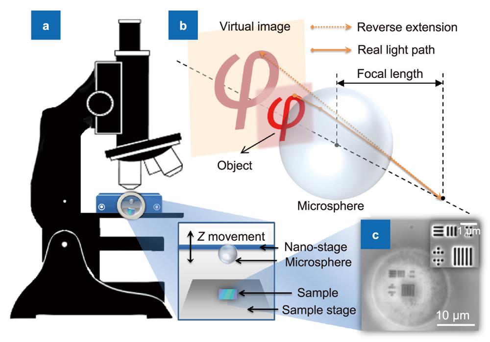
In our case, the microsphere is positioned above the sample surface to form an enlarged virtual image. A conventional microscope system is used to capture the virtual image provided by the microsphere. The schematic illustration of this system is shown in
Fig. 1a
. In this case, the microsphere functions similar to a ball lens. Its dominating effect is to refract the incident light so it can magnify the image
25
-
27
. Such magnification of the image can be described by the equation
30
,
31
:

Figure 1.(
a
) Schematic diagram of the remote mode optical microsphere setup. (
b
) Mechanism to illustrate the enlarged virtual image by the microsphere. (
c
) Optical image captured by this system (Sample: semiconductor testing sample; scale bar: 10 μm; imaged by a 20 μm silica microsphere compiled to an oil-immersion optical microscope with a 100× objective lens, NA=1.4). Inset: SEM image (scale bar: 1 μm).
where
β
is the overall magnification of the microsphere,
β1
the contribution from the upper surface of the microsphere, and
β2
the contribution from the lower surface. When the dimension of the microsphere is 10 times larger than the wavelength of the light, we can apply the principles in the geometrical optics to rewrite equation (1) in the forms of the microsphere parameters:
where
n1
and
n2
are the refractive indices of the environment and microsphere, respectively;
d
the distance between the object and the lower surface of the microsphere;
r
the radius of the microsphere. The derivation is shown in the Supplementary information. In the first experiment presented in the next section, equation (2) is verified with a microsphere of 400 μm diameter. However, Equation (2) needs to be further modified when the dimension of the microsphere is reduced. As the operation of the microsphere is in a small area close to the sample, the gap between the sample and the microsphere is smaller than 10 times of the wavelength. In our experiments, the object is placed at a distance within the back focal length (BFL) of the microsphere. For smaller microspheres, they need to be positioned close to the object surface for their reduced BFL. In our second experiment, the diameter of the microspheres is around 20 μm. The distance between the bottom of the microsphere and the sample surface ranges from 500 nm to 1 μm, which is optimized for different samples to achieve clear surface feature imaging. For our light illumination condition, this working distance is in the transition zone between the optical near field and far field. While the upper surface can still be described by the Snell's Law, for the lower surface, corrections need to be made on equation (2) for the case of light properties in this transition zone. Hence, equation (2) and the overall magnification (
β
') is further modified by a factor
k
:
where
k
is the modification factor providing the correction as this system cannot be fully described by the principles of geometric optics in this transition zone
25
,
30
,
31
. For this case, the imaging theory predicts an enlarged virtual image. The position of this virtual image is below the surface of the object, which represents a key feature of the imaging process (illustrated in
Fig. 1b
). Such a key feature is verified in our experiments (details presented in Supplementary information Videos). In addition to the imaging magnification, the microsphere can also resolve fine features more clearly as described in the previous work
25
. These mechanisms explain why the microsphere can magnify the object. It also reveals that the key feature of our method is to provide an enlarged virtual image and enhance the observation power of nearly all optical microscopes by the magnification factor (
β
) in theory (
Fig. 1c
). Furthermore, such theoretical understanding provides the guidance to identify and optimize the important parameters in the imaging process. Besides the selection of the microsphere, equation (3) also indicates that it is crucial to lift the microsphere up and work in remote mode and control the distance between the microsphere and the sample since the magnification factor (
β
) is directly related to
d
. Based on this knowledge, we design a patented setup with an accurate control of 1 nm of the microsphere position
32
. This setup is also highly flexible and compatible for liquid environments with different refractive indices, which makes it possible to characterize various samples as described in the following sections.
Firstly, we apply a microsphere of 400 μm diameter to a 20× conventional objective lens to verify equation (2), which studies the functionality of the microsphere in optical far field (
Fig. 2
). We designed a universal setup as shown in
Fig. 2a
. The gap between the microsphere and the object was measured to be 65 μm, which was 100 times larger than the central wavelength of the incident light. As discussed in the previous section, the key for this method is the remote microsphere integrated with the conventional objective lens. A special adapter is designed to mount the microsphere setup on the objective lens (
Fig. 2c
). The distance between the objective lens and the microsphere can be controlled precisely by a stepper motor on the mechanical frame (more details in Method section). With this setup, we can easily adjust the relative positions of the object, microsphere, and objective lens.
Fig. 2d
shows the imaging results by this setup. It is obvious that the 20× conventional objective lens with the microsphere achieves the observation power similar to a 50× objective lens. The key feature in these images is the cell wall, which is marked in black circles for comparison. These imaging results verify the magnification mechanism of the microsphere. With these novel optical nano-scope strategies, we can build a completely new universal nano-imaging platform to provide general purpose imaging solutions. This setup can be widely applied to conventional microscope-based systems. Such cost-efficient upgrade was successfully tested to characterize biological samples (onion cells). Due to the high stability of this adapter, it is able to scan through the surface and integrate separate images together as shown in
Fig. 2b
. There is almost no aberration at the central region of the virtual image. Without sacrificing the observation capability and imaging quality, the field of view is greatly extended to 125 μm × 125 μm via this image integration (theoretically there is no limitation on the scanning area while a larger area takes longer time to scan). Such a broad field of view is sufficient to study the
in vivo
reactions between cells and multicellular mechanisms
33
. These experimental results demonstrate the rich opportunities to upgrade the most widely used low-resolution microscope from 20× to 50 ~100× objective lens depending on the settings. This technology can benefit many people, including medical researchers, integrated electronics industry workers, doctors, and students.
Figure 2.(
a
) Schematic of the design of the universal lens adaptor for the microsphere (silica microsphere with 400 μm diameter attached on a 20× objective lens. Characterization was done in ambient air and distance between the onion cell and the microsphere is ~65 μm, with white light illumination). (
b
) Integrated image of onion cells (scale bar: 20 μm). (
c
) Optical image of the universal sample adaptor after integration. (
d
) Comparison of the optical images by three optical lenses: the 20× objective lens (left, scale bar: 20 μm); 20× objective lens with the microsphere (middle, which is our nanoscope design, scale bar: 8 μm); and 50× objective lens (right, scale bar: 8 μm).
While the first experiment focuses on the far field imaging, in the second experiment, we move forward to explore the magnification of the microsphere working in the transition zone between the far field and near field. For the conventional optical microscope equipped with a 100× oil-immersion lens and confocal noise reduction, it can resolve features of 200 nm size (such as Nikon Eclipse Ni-E). To demonstrate the resolving power of our system, we attach the microsphere (diameter ~20 μm) to a conventional microscope with a 100× objective lens under the oil-immersion mode. In this case, the microsphere is controlled flexibly by our patented technology to keep it remote from the surface. Such technology ensures the precise control of 1 nm motion step on the position of the microsphere, which is important to achieve fine tuning required for nano-imaging. An array of paired nano-dots (
Fig. 3a
) is fabricated for characterization. Each pair of nano-dots is separated by a nano-gap of 23~31 nm. Compared with the images captured by the conventional system (
Fig. 3b
), our system can distinguish each pair of the nano-dots clearly (
Fig. 3c
), with the smallest nano-gap down to 23 nm. In this approach, a remote microsphere, which functions as a tiny lens, upgrades the observation power of a conventional microscope to a level comparable to vacuum-based table-top scanning electron microscopes (HITACHI TM3000, 30 nm resolution). To further investigate the observation capability on complicated arbitrary nanostructures, we fabricate a 2 × 2 μm "nano-rose" pattern on a ~100 nm thick Cr film deposited on a quartz substrate. The SEM picture of this "nano-rose" pattern is shown in
Fig. 3d
. It possesses arbitrary-shaped nano-grooves in between the written structures with typical sizes of 50 ~ 60 nm. As a reference, observing such a complex structure under the conventional microscope (100× oil-immersion objective lens) only obtains a blurred image, since the nano-grooves are not readily resolved (
Fig. 3e
). When we apply our remote microsphere setup to the same microscope system, the nano-grooves are clearly displayed (
Fig. 3f
), demonstrating its much stronger resolving power of features below 100 nm. For the imaging of the nano-rose, the microsphere with larger diameter (27 μm) is chosen to contain the entire "nano-rose" pattern in its central region of view. The depth of focus (DOF) was measured to be ~500 nm for this setup. The beauty of this invention is that the microsphere is suspended remotely from the sample surface (details see Supplementary information). This non-contact feature enables the imaging of various samples while preventing surface contamination in the previous methods by contacting the microsphere to the sample surfaces, which is crucial for general purpose imaging
1
,
2
. One example is the imaging of a magnetic head on a hard disc drive from a production line (
Fig. 3g
), which is characterized in real-time, ambient air and non-contact mode. The 77 nm gap between the metal probe and the body is totally not resolvable for the conventional oil-immersion microscope (
Fig. 3h
). Nevertheless, a clear gap is observed by our microsphere nanoscope (
Fig. 3i
). This experiment result reveals its great potential applications in the real-time high-precision quality inspection of industrial products. More imaging results are summarized in Supplementary information.
Figure 3.(
a
~
c
) Imaging of nano-dot pairs with nano-gap on a Si wafer. (
a
) SEM image of the samples, showing sizes of nano-gaps in between each pair of nano-dots. (
b
) Imaging of the samples by an oil-immersion microscope (neighboring nano-dots cannot be resolved clearly). (
c
) Neighboring separated nano-dots are resolved clearly by a microsphere with 20 μm diameter. The back dash line in (
c
) indicates the line cut (the intensity analysis is presented in supplementary materials). (
d
~
f
) Imaging of samples with complex features (the "nano-rose"). (
d
) Zoomed-in SEM image with size notations, it shows that the typical line width of the structure is ~140 nm, and separated by nano-grooves with a typical size ranging from 50~60 nm. (
e
) Imaging result by the oil-immersion optical microscope. (
f
) Image under the 27μm microsphere in scanning mode. The diameter of the microsphere is larger in order to contain the entire nano-rose in the central region. (Compared to the microsphere used for the imaging of nano-dots, the microsphere with a larger diameter is chosen to ensure the entire nano-rose pattern is in the central region of the microsphere. Inset: zoomed-in image under the microsphere). (
g
~
i
) Imaging of a magnetic head in a hard disc drive from the production line. (
g
) SEM image of the magnetic head, with a nano-gap of 77 nm. (
h
) Imaging by a conventional oil-immersion microscope. (
i
) Imaging by the microsphere nanoscope in non-contact mode. The three columns represent images obtained by SEM, oil-immersion optical microscope (100×, NA 1.4), and microsphere nanoscope, respectively.
Conclusions
In summary, we invent a new microsphere nanoscope with a benchmark nano-scale observation power down to 23 nm. This method has many unique advantages, such as non-contact, dynamic, non-invasive, and capable to work in both ambient air and liquid environments. Sufficient theoretical understanding is presented to build and adjust such nano-imaging platform. Sub-100 nm observation power is demonstrated on the lab-fabricated nano-dots array and magnetic head sample from industry. Furthermore, since our design can be applied flexibly to most of the conventional microscopes, it is highly promising to integrate our method with other microscope-involved techniques. There is no limitation on the light condition. Both the light-field imaging and dark-field imaging are feasible. Based on these points, we believe that this advance in the microscope is beneficial for a broad range of disciplines.
Methods
The key to realize the high-quality nano-imaging results is to adjust the microsphere accurately according to different imaging conditions. From equations (2) and (3), it can be concluded that the two critical parameters for imaging are the BFL and object distance
d
. In this section, we shall discuss the strategy to optimize the nano-imaging quality. The BFL primarily depends on the refractive index and the diameter of the microsphere
25
-
27
. The magnification capability of a microsphere increases with the refractive index in general. High refractive index dielectric material with almost zero loss is preferred. Compared with other nano-imaging methods which suffer from high loss issues (such as the metal-based supercritical lens and near-field optical microscope), the choice of low-loss material is a favorable feature for optical imaging. However, it is worth mentioning that when the microsphere has a refractive index larger than 2.0 in ambient air, its focal point is inside the microsphere
30
. The diameter of the microsphere also affects the BFL. In the first experiment of the far field imaging, the BLF can be directly calculated according to geometrical optics. In the second imaging experiment in the transition zone between the far field and near field, in which the microsphere has a diameter of ~20 μm, numerical methods need to be applied to study the optimized value
25
,
27
. Then, the next step is to adjust the distance between the microsphere and the objective lens to ensure that the objective lens captures the enlarged virtual image clearly in the remote mode. For each object-to-microsphere distance, the parameters can be found by scanning the objective lens at different heights above the microsphere setup. More details can be found in Supplementary information.
Acknowledgements
We thank L Yang, J Liu, Z C Chen and J Z Ling for their help. We are grateful for financial supports from the A*STAR, SERC 2014 Public Sector Research Funding (PSF) Grant (SERC Project No. 1421200080).
Author contributions
M H Hong proposed the original idea and supervised the project. Y Zhou and M X Wu fabricated the samples and performed the measurements. L W Chen and M H Hong analysed the results and co-wrote the paper. All authors commented on the manuscript.
Competing interests
The authors declare no competing financial interests.
Supplementary information
Section 1: Comparison of the imaging techniques from biological aspects
Section 2: Photo gallery of the microsphere imaging results
Section 3: Theoretical derivation of the imaging principles
Section 4: Experiments to demonstrate the virtual image
Section 5: Optimization procedure for the microsphere imaging
Section 6: Real-time imaging results
Section 7: Line-cut analysis for nano-dots in
Fig. 3
Video S1: The optimized location of the microsphere
Video S2: The nano-dots' dynamic imaging results
Video S3: The nano-rose' s dynamic imaging results
Video S4: The imaging process of the semiconductor testing chip
References
[1] J Clevelanda, T J Montvillea, I F Nesb, M L Chikindas. Bacteriocins: safe, natural antimicrobials for food preservation. Int J Food Microbiol, 71, 1-20(2001).
[2] O'Mara W C, Herring R B, Hunt L P. Handbook of Semiconductor Silicon Technology
(Noyes Publications, 1990)..
[3] S Bradbury. The microscope: past and present(1968).
[4] F Qin, K Huang, J F Wu, J H Teng, C W Qiu et al. A supercritical lens optical label-free microscopy: sub-diffraction resolution and ultra-long working distance. Adv Mater, 29, 1602721(2017).
[5] F Qin, L Ding, L Zhang, F Monticone, C C Chum et al. Hybrid bilayer plasmonic metasurface efficiently manipulates visible light. Sci Adv, 2, 1-9(2016).
[6] F Qin, K Huang, J F Wu, J Jiao, X G Luo et al. Shaping a subwavelength needle with ultra-long focal length by focusing azimuthally polarized light. Sci Rep, 5, 9977(2015).
[7] Y T Wang, B H Cheng, Y Z Ho, Y C Lan, P G Luan et al. Gain-assisted hybrid-superlens hyperlens for nano imaging. Opt Express, 20, 22953-22960(2012).
[8] Y H Lin, D P Tsai. Near-field scanning optical microscopy using a super-resolution cover glass slip. Opt Express, 20, 16205-16211(2012).
[9] T Fukaya, D Buchel, S Shinbori, J Tominaga, N Atoda et al. Micro-optical nonlinearity of a silver oxide layer. J Appl Phys, 89, 6139-6144(2001).
[10] Y Li, X Li, L W Chen, M B Pu, J J Jin et al. Orbital angular momentum multiplexing and demultiplexing by a single metasurface. Adv Opt Mater, 5, 1600502(2017).
[11] X Li, L W Chen, Yang Li, X H Zhang, M B Pu et al. Multicolor 3D meta-holography by broadband plasmonic modulation. Sci Adv, 2, e1601102(2016).
[12] B Huang, W Q Wang, M Bates, X W Zhuang. Three-dimensional super-resolution imaging by stochastic optical reconstruction microscopy. Science, 319, 810-813(2008).
[13] E Betzig, G H Patterson, R Sougrat, O W Lindwasser, S Olenych et al. Imaging intracellular fluorescent proteins at nanometer resolution. Science, 313, 1642-1645(2006).
[14] G Binnig, H Rohrer. Scanning tunneling microscopy. IBM J Res Dev, 4, 355-369(1986).
[15] X Luo. Principles of electromagnetic waves in metasurfaces. Sci China: Phys Mech Astron, 58, 594201(2015).
[16] Y T Wang, B H Cheng, Y Z Ho, Y C Lan, P G Luan et al. Optical hybrid-superlens hyperlens for superresolution imaging. IEEE J Sel Top Quantum Electron, 19, 4601305(2013).
[17] B H Cheng, Y C Lan, D P Tsai. Breaking optical diffraction limitation using optical hybrid-super-hyperlens with radially polarized light. Opt Express, 21, 14898-14906(2013).
[18] X Luo, T Ishihara. Surface plasmon resonant interference nanolithography technique. Appl Phys Lett, 84, 4780-4782(2004).
[19] D Tang, C Wang, Z Zhao, Y Wang, M Pu et al. Ultrabroadband superoscillatory lens composed by plasmonic metasurfaces for subdiffraction light focusing. Laser Photonics Rev, 9, 713-719(2015).
[20] . So Much More to Know. Science, 309, 78-102(2005).
[21] N Yu, P Genevet, M A Kats, F Aieta, J -P Tetienne et al. Light propagation with phase discontinuities: generalized laws of reflection and refraction. Science, 334, 333-337(2011).
[22] M Pu, X Li, X Ma, Y Wang, Z Zhao et al. Catenary optics for achromatic generation of perfect optical angular momentum. Sci Adv, 1, e1500396(2015).
[23] X Li, M Pu, Y Wang, X Ma, Y Li et al. Dynamic control of the extraordinary optical scattering in semicontinuous 2d metamaterials. Adv Opt Mater, 4, 659-663(2016).
[24] Z B Wang, W Guo, L Li, B Luk'yanchuk, A Khan, Z Liu et al. Optical virtual imaging at 50 nm lateral resolution with a white-light nanoscope. Nat Commun, 2, 218(2011).
[25] H Yang, R Trouillon, G Huszka, M A M Gijs. Super-resolution imaging of a dielectric microsphere is governed by the waist of its photonic nanojet. Nano Lett, 16, 4862-4870(2016).
[26] A Darafsheh, C Guardiola, A Palovcak, J C Finlay, A Cárabe. Optical super-resolution imaging by high-index microspheres embedded in elastomers. Opt Lett, 40, 5-8(2015).
[27] F F Wang, L Q Liu, P Yu, Z Liu, H B Yu et al. Three-dimensional super-resolution morphology by near-field assisted white-Light interferometry. Sci Rep, 6, 24703(2016).
[28] A Darafsheh, N I Limberopoulos, J S Derov, D E Walker, V N Astratov. Advantages of microsphere-assisted super-resolution imaging technique over solid immersion lens and confocal microscopies. Appl Phys Lett, 104, 61117(2014).
[29] F F Wang, L Q Liu, H B Yu, Y D Wen, P Yu et al. Scanning superlens microscopy for non-invasive large field-of-view visible light nanoscale imaging. Nat Commun, 7, 13748(2016).
[30] M Born, E Wolf. Principles of optics; electromagnetic theory of propagation, interference, and diffraction of light(1975).
[31] Soroko L M.. Meso-optics, foundations and applications
(World Scientific, 1996)..
[32] Hong Wu M.. Immersion Nanoscope Lens Assembly Chip for Super-resolution Imaging. PRV 10201608343Y (2016)..
[33] G M Dunny, T J Brickman, M Dworkin. Multicellular behavior in bacteria, communication, cooperation, competition and cheating. Bio Essays, 30, 296-298(2008).