• Photonics Research
  • Vol. 5, Issue 2, A35 (2017)
Mohamed Sufyan Islim1、*, Ricardo X. Ferreira2, Xiangyu He2, Enyuan Xie2, Stefan Videv3, Shaun Viola4, Scott Watson4, Nikolaos Bamiedakis5, Richard V. Penty5, Ian H. White5, Anthony E. Kelly4, Erdan Gu2, Harald Haas3, and Martin D. Dawson2
Author Affiliations
  • 1Li–Fi R&D Centre, the University of Edinburgh, Institute for Digital Communications, King’s Buildings, Mayfield Road, Edinburgh EH9 3JL, UK
  • 2Institute of Photonics, Department of Physics, University of Strathclyde, Glasgow G1 1RD, UK
  • 3Institute for Digital Communications, Li–Fi R&D Centre, the University of Edinburgh, King’s Buildings, Mayfield Road, Edinburgh EH9 3JL, UK
  • 4School of Engineering, University of Glasgow, Glasgow G12 8LT, UK
  • 5Centre for Advanced Photonics and Electronics, Electrical Engineering Division, Department of Engineering, University of Cambridge, Cambridge CB3 0FA, UK
  • show less
    DOI: 10.1364/PRJ.5.000A35 Cite this Article Set citation alerts
    Mohamed Sufyan Islim, Ricardo X. Ferreira, Xiangyu He, Enyuan Xie, Stefan Videv, Shaun Viola, Scott Watson, Nikolaos Bamiedakis, Richard V. Penty, Ian H. White, Anthony E. Kelly, Erdan Gu, Harald Haas, Martin D. Dawson. Towards 10  Gb/s orthogonal frequency division multiplexing-based visible light communication using a GaN violet micro-LED[J]. Photonics Research, 2017, 5(2): A35 Copy Citation Text show less
    Plan view micrographs of the segmented micro-LED arrays. The magnified micrographs on the right show the array configuration and individual pixel design. A diagram is also included noting the inner and outer pixels (dimensions in micrometers).
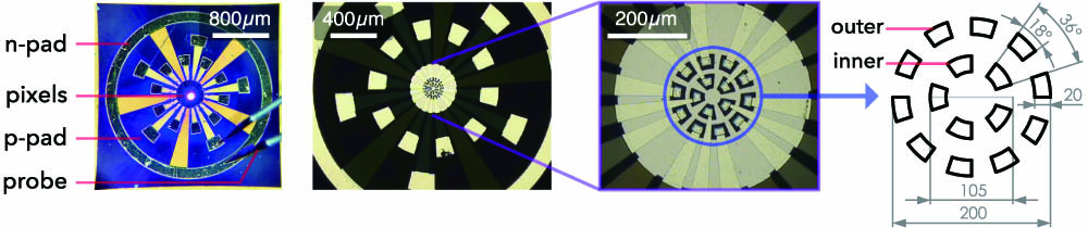
    Fig. 1. Plan view micrographs of the segmented micro-LED arrays. The magnified micrographs on the right show the array configuration and individual pixel design. A diagram is also included noting the inner and outer pixels (dimensions in micrometers).
    Combined current–voltage (I–V), left, and luminescence–current (L–I), right, characteristics of both inner and outer pixels. The inset shows the emission spectrum of an inner pixel at 50 mA.
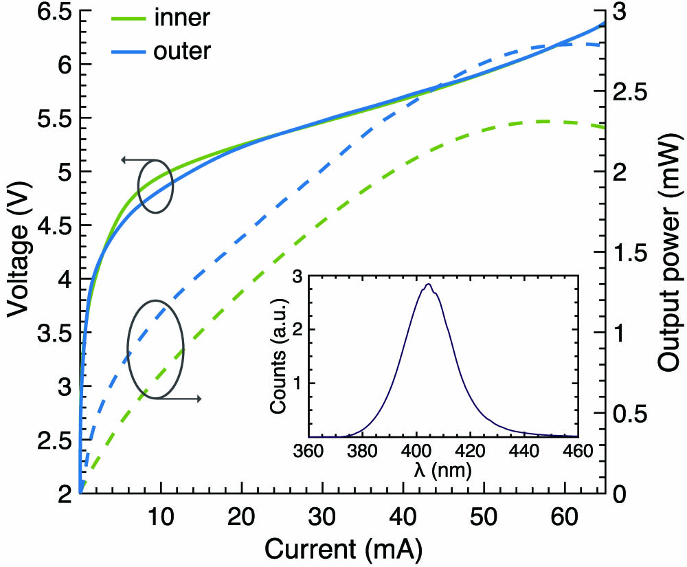
    Fig. 2. Combined current–voltage (I–V), left, and luminescence–current (L–I), right, characteristics of both inner and outer pixels. The inset shows the emission spectrum of an inner pixel at 50 mA.
    Small signal frequency response for the inner pixel at 5 and 50 mA. The inset shows 6 dB E-O bandwidth at different values for the current density J, corresponding to DC-bias values of 5–50 mA.
    Fig. 3. Small signal frequency response for the inner pixel at 5 and 50 mA. The inset shows 6 dB E-O bandwidth at different values for the current density J, corresponding to DC-bias values of 5–50 mA.
    Block diagram for OFDM transmitter and receiver.
    Fig. 4. Block diagram for OFDM transmitter and receiver.
    (a) Bit loading and channel capacity per subcarrier, both given in bits per subcarrier. (b) Energy loading per subcarrier.
    Fig. 5. (a) Bit loading and channel capacity per subcarrier, both given in bits per subcarrier. (b) Energy loading per subcarrier.
    Statistical CDF for different QAM constellation sizes realized at BER=2.3×10⁻³, below the FEC target.
    Fig. 6. Statistical CDF for different QAM constellation sizes realized at BER=2.3×10³, below the FEC target.
    Experimental setup. (a) Schematic setup of the experiment showing the optical system, AWG, oscilloscope, amplifier, attenuator, and Bias-tee. (b) Photograph of the optical system showing the micro-LED, the optical lens system, and the photoreceiver.
    Fig. 7. Experimental setup. (a) Schematic setup of the experiment showing the optical system, AWG, oscilloscope, amplifier, attenuator, and Bias-tee. (b) Photograph of the optical system showing the micro-LED, the optical lens system, and the photoreceiver.
    Experimentally obtained results and theoretical bounds of data rate and BER versus different dimming levels at a modulation depth of VPP=2.36 V. The values for the received optical power correspond to DC-bias values ranging from 10 to 40 mA.
    Fig. 8. Experimentally obtained results and theoretical bounds of data rate and BER versus different dimming levels at a modulation depth of VPP=2.36  V. The values for the received optical power correspond to DC-bias values ranging from 10 to 40 mA.
    Theoretical bounds on the data rate versus BER for different dimming levels at a modulation depth of VPP=2.36 V. The values for the received optical power correspond to DC-bias values ranging from 10 to 40 mA. Filled markers denote experimental results.
    Fig. 9. Theoretical bounds on the data rate versus BER for different dimming levels at a modulation depth of VPP=2.36  V. The values for the received optical power correspond to DC-bias values ranging from 10 to 40 mA. Filled markers denote experimental results.
    SNR versus frequency for different modulation depths at DC-bias current IDC=30 mA. The values for the modulation signal swings correspond to feeding the micro-LED with varying power levels from 5.85 to 11.78 dBm.
    Fig. 10. SNR versus frequency for different modulation depths at DC-bias current IDC=30  mA. The values for the modulation signal swings correspond to feeding the micro-LED with varying power levels from 5.85 to 11.78 dBm.
    Data rates versus BER for the experimentally obtained and the theoretical bounds at DC-bias current IDC=30 mA corresponding to Popt=−2.6 dBm and modulation depth VPP=3.88 V.
    Fig. 11. Data rates versus BER for the experimentally obtained and the theoretical bounds at DC-bias current IDC=30  mA corresponding to Popt=2.6  dBm and modulation depth VPP=3.88  V.
    Distance versus received optical power (left) and data rate (right). (a) Study I with transmitter and receiver lenses and Study II with transmitter lens only. (b) Study III with receiver lens only and Study IV without any optics.
    Fig. 12. Distance versus received optical power (left) and data rate (right). (a) Study I with transmitter and receiver lenses and Study II with transmitter lens only. (b) Study III with receiver lens only and Study IV without any optics.
    Received optical power distribution in dBm as a function of vertical–horizontal displacements. (a) Study I at a distance of 369 cm; (b) Study I at a distance of 525 cm; (c) Study II at a distance of 104 cm; (d) Study II at a distance of 147 cm; (e) Study III at a distance of 4.7 cm; (f) Study III at a distance of 6.6 cm; (g) Study IV at a distance of 1.3 cm; (h) Study IV at a distance of 1.9 cm.
    Fig. 13. Received optical power distribution in dBm as a function of vertical–horizontal displacements. (a) Study I at a distance of 369 cm; (b) Study I at a distance of 525 cm; (c) Study II at a distance of 104 cm; (d) Study II at a distance of 147 cm; (e) Study III at a distance of 4.7 cm; (f) Study III at a distance of 6.6 cm; (g) Study IV at a distance of 1.3 cm; (h) Study IV at a distance of 1.9 cm.
    Mohamed Sufyan Islim, Ricardo X. Ferreira, Xiangyu He, Enyuan Xie, Stefan Videv, Shaun Viola, Scott Watson, Nikolaos Bamiedakis, Richard V. Penty, Ian H. White, Anthony E. Kelly, Erdan Gu, Harald Haas, Martin D. Dawson. Towards 10  Gb/s orthogonal frequency division multiplexing-based visible light communication using a GaN violet micro-LED[J]. Photonics Research, 2017, 5(2): A35
    Download Citation