Mohamed Sufyan Islim1、*, Ricardo X. Ferreira2, Xiangyu He2, Enyuan Xie2, Stefan Videv3, Shaun Viola4, Scott Watson4, Nikolaos Bamiedakis5, Richard V. Penty5, Ian H. White5, Anthony E. Kelly4, Erdan Gu2, Harald Haas3, and Martin D. Dawson2
1Li–Fi R&D Centre, the University of Edinburgh, Institute for Digital Communications, King’s Buildings, Mayfield Road, Edinburgh EH9 3JL, UK
2Institute of Photonics, Department of Physics, University of Strathclyde, Glasgow G1 1RD, UK
3Institute for Digital Communications, Li–Fi R&D Centre, the University of Edinburgh, King’s Buildings, Mayfield Road, Edinburgh EH9 3JL, UK
4School of Engineering, University of Glasgow, Glasgow G12 8LT, UK
5Centre for Advanced Photonics and Electronics, Electrical Engineering Division, Department of Engineering, University of Cambridge, Cambridge CB3 0FA, UK
Mohamed Sufyan Islim, Ricardo X. Ferreira, Xiangyu He, Enyuan Xie, Stefan Videv, Shaun Viola, Scott Watson, Nikolaos Bamiedakis, Richard V. Penty, Ian H. White, Anthony E. Kelly, Erdan Gu, Harald Haas, Martin D. Dawson. Towards 10 Gb/s orthogonal frequency division multiplexing-based visible light communication using a GaN violet micro-LED[J]. Photonics Research, 2017, 5(2): A35
Copy Citation Text
Visible light communication (VLC) is a promising solution to the increasing demands for wireless connectivity. Gallium nitride micro-sized light emitting diodes (micro-LEDs) are strong candidates for VLC due to their high bandwidths. Segmented violet micro-LEDs are reported in this work with electrical-to-optical bandwidths up to 655 MHz. An orthogonal frequency division multiplexing-based VLC system with adaptive bit and energy loading is demonstrated, and a data transmission rate of 11.95 Gb/s is achieved with a violet micro-LED, when the nonlinear distortion of the micro-LED is the dominant noise source of the VLC system. A record 7.91 Gb/s data transmission rate is reported below the forward error correction threshold using a single pixel of the segmented array when all the noise sources of the VLC system are present.
The increasing demands of communication services are challenging radio frequency (RF) wireless communications technologies. The overall number of networked devices is expected to reach 26.3 billion in 2020 [1]. Visible light communication (VLC) is a promising solution to the limited availability of the RF spectrum as the visible light spectrum offers abundant bandwidth that is unlicensed and free to use. VLC improves the spectral efficiency per unit area, which enhances the quality of service in crowded environments and allows for secure and localized services to be provided.
General lighting is under a rapid transformation to become semiconductor based due to huge energy savings. This transformation has already enabled applications such as active energy consumption control and color tuning. Solid state lighting devices such as gallium nitride (GaN)-based inorganic light emitting diodes (LEDs) are ubiquitous power-efficient devices to enable illumination and communications. Commercially available LEDs have a limited frequency response due to the yellow phosphor coating on top of the blue LED chips. However, the slow response of the yellow phosphor can be filtered out using a blue filter in front of the receiver. Recent results for VLC using a phosphorescent white LED with adaptive bit and energy loading were reported at 2.32 Gb/s aided by a two-staged linear software equalizer [2].
Micro-LEDs are promising candidates in enabling lighting as a service (LaaS) and Internet of things (IoT). The introduction of micro-LEDs has enabled high-performance value-added lighting functions such as VLC and indoor positioning and tracking [3]. Micro-LEDs are known for their small active areas enabling high current density injection, which drives the modulation bandwidth to hundreds of megahertz [4,5]. At 450 nm, micro-LEDs have set the standard for high-speed VLC. A 60 μm diameter pixel has achieved 3 Gb/s [6], and more recently a single pixel of a new segmented array has demonstrated 5 Gb/s [7]. The novel micro-LEDs emitting at 400 nm featured in the current work offer a number of advantages over the 450 nm devices previously reported [7]. From typical trends concerning the internal quantum efficiency (IQE) of indium GaN-based active regions, comparable IQEs are expected at 400 and 450 nm, whereas the IQE decreases steeply at shorter emission wavelengths [8]. For generation of white light for illumination, the use of violet-emitting LEDs exciting tricolor (red, green, and blue) phosphors also offers advantages over the widely used method of combining blue direct LED emission with a yellow-emitting phosphor. These include much superior color rendering indices [9,10] and the absence of a direct blue component, which has proven to be disruptive to the human circadian rhythm [11]. The micro-LED die shapes employed in this work are also expected to be advantageous for efficient light extraction, by analogy with previous designs employing non-circular emitting areas [12].
Sign up for Photonics Research TOC. Get the latest issue of Photonics Research delivered right to you!Sign up now
VLC is enabled by incoherent illumination from the light sources. Therefore, only real and positive modulating waveforms can be realized. Single carrier modulation schemes such as on–off keying (OOK), pulse amplitude modulation (PAM), and pulse width modulation (PWM) are straightforward to implement. However, the performance of these modulation schemes degrades as the transmission speed increases due to the increased inter-symbol interference (ISI). Equalization techniques can be used to improve the system performance at significant computation cost [13]. Multi-carrier modulation techniques such as orthogonal frequency division multiplexing (OFDM) are promising candidates for VLC. Computationally efficient single-tap equalizers are straightforward to realize in OFDM. Adaptive bit and energy loading in OFDM allows the channel utilization to approach the information capacity limit. In addition, multiple access can be easily supported in OFDM by assigning groups of subcarriers to multiple users, which is known as orthogonal frequency division multiple access (OFDMA).
Previously, a 40 μm diameter micro-LED at 405 nm achieved a data rate of 3.32 Gb/s at an optical power of 2.5 mW with electrical–optical bandwidth up to 307 MHz [14]. In this paper, we present a high bandwidth VLC link at 400 nm. The emitter consists of a single pixel of the segmented micro-LED array design introduced in Ref. [7]. This device achieves 2.3 mW of optical output power while maintaining an electrical-to-optical (E-O) bandwidth of 655 MHz. A VLC system is realized with a modulation bandwidth of 1.81 GHz, evaluated beyond the 3 dB bandwidth of the system. A transmission rate of 11.95 Gb/s is presented, when the nonlinear distortion noise of the micro-LED is the major source of noise in the system. A record transmission rate at 7.91 Gb/s is presented when all the noise sources of the VLC system are considered.
2. VIOLET MICRO-LED
A. Design and Fabrication
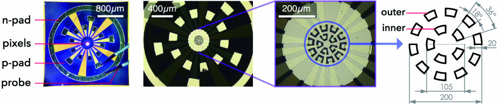
The design of standard GaN LEDs is based on a large-area chip assembled on a package that maximizes heat extraction through an n-pad at the bottom for a flip-chip configuration. This creates two limitations: a large capacitance due to the package contact area and an upper limit on the current density due to the rapid self-heating of a large-area chip. The design and fabrication process of the micro-LED array used in this work is as reported in our previous work [7]. It consists of two circular micro-LED arrays, an inner and an outer, containing 5 and 10 pixels, respectively. Originally designed to match the geometry of plastic optical fiber, the inner and outer pixels have active areas of 435 and , respectively. This compares with the active area for the 405 nm device in Ref. [14]. Figure 1 shows optical images of this micro-LED array, together with a schematic of the pixel layout.
The wafer used in this work is for a commercially available GaN-based LED emitting at 400 nm. In order to fabricate these arrays, micro-LEDs emitters are etched by inductively coupled plasma to expose -type GaN. An annealed layer is used as a metal contact to -type GaN. Each emitter is isolated by a layer of . The metallization on the -type GaN is formed by depositing a Ti/Au metal bilayer, which fills the area between each micro-LED and enables an improved current spreading. This bilayer connects each micro-LED emitter in order to individually address them. The micro-LED array allows increasing the total output power with minimal reduction in performance due to mutual heating between pixels. The low optical power per pixel in micro-LEDs is a challenge when combined illumination and communication is considered. This problem can be addressed by using large arrays of pixels, where a system capable of handing the communication link over multiple pixels can be designed to reduce the duty cycle, reduce the junction temperature on individual pixels, and maintain high efficiency. These investigations are subject to future work.
Figure 1.Plan view micrographs of the segmented micro-LED arrays. The magnified micrographs on the right show the array configuration and individual pixel design. A diagram is also included noting the inner and outer pixels (dimensions in micrometers).
The electrical performance of the micro-LED arrays was measured by a semiconductor analyzer (HP 4155). The optical power of the arrays under direct current (DC) conditions was measured using a Si detector placed in close proximity to the polished sapphire substrate. A spectrometer and a charge coupled device detection system were used for the collection of electroluminescence spectra. The small signal frequency response was measured by a network analyzer with a 20 mV alternating current (AC) frequency sweep signal combined in a bias-tee with a DC-bias current ranging from 5 to 50 mA. The optical response was collected by a lens system and focused onto a fast photodiode (PD) and fed to the network analyzer. All the measurements were performed at room temperature with the device directly probed on chip with a high-speed probe to guarantee minimal parasitic effects.
1. I–V and L–I Characteristics
Devices with linear luminescence–voltage (L–V) characteristics and high optical power allow for a large dynamic range that can accommodate large swings of modulating signals, and this subsequently improves the signal-to-noise ratio (SNR) of the VLC system. The current–voltage (I–V) and luminescence–current (L–I) characteristics for the micro-LED are presented in Fig. 2. The pixels present a shunt resistance responsible for a subthreshold turn-on; this is attributed to damaged regions in the junction and by surface imperfections. Differences between the inner and the outer pixels are minimal in I–V with a series resistance of and and threshold turn-on voltage of 4.60 and 4.64 V for the inner and outer pixels, respectively. In terms of optical power, at the roll-over point, the outer pixels achieve a maximum of 2.79 mW, 17% higher than the inner pixel, which is expected given the larger active area. This compares to 2.5 mW from a pixel at 405 nm with a 2.88 times larger active area [14]. The improvement in the optical power is due to the improved -type contact, resulting in 50% higher optical power compared to Ref. [14]. In addition, the commercially supplied wafer for this micro-LED gives better IQE.
Figure 2.Combined current–voltage (I–V), left, and luminescence–current (L–I), right, characteristics of both inner and outer pixels. The inset shows the emission spectrum of an inner pixel at 50 mA.
The frequency response from 100 kHz to 1.5 GHz for the lowest and highest bias currents of the testing set are presented in Fig. 3. At 1.5 GHz modulation, the pixels do not reach the noise floor of the system, thus providing a large useful bandwidth for data transmission. The calculated E-O bandwidth against current density is shown in the inset of Fig. 3 for the set of bias currents covering the full operating range. The current densities for these pixels are in line with what was previously seen at 450 nm [7], meaning that the pixels achieve similar bandwidth at the same current density. This is also compared with 307 MHz bandwidth for the 405 nm device in Ref. [14]. The improvement in bandwidth over [14] is due to the smaller active area of the device that allowed higher current density and shorter carrier lifetime. With a bandwidth of 655 MHz for the inner pixel, to the authors’ best knowledge, this micro-LED has the highest bandwidth yet shown in the violet wavelength band.
Figure 3.Small signal frequency response for the inner pixel at 5 and 50 mA. The inset shows 6 dB E-O bandwidth at different values for the current density , corresponding to DC-bias values of 5–50 mA.
Multiple variants of OFDM have been proposed for VLC [15]. Conventional OFDM waveforms are both complex and bipolar; however, Hermitian symmetry can be imposed on the OFDM subcarrier frame to realize real-valued OFDM waveforms, , where is the OFDM frame size, and is the subcarrier index. In addition, subcarriers at and are set to zero. DC-biased optical OFDM (DCO-OFDM) uses a DC bias to shift most of the negative real-valued OFDM samples into positive. The block diagram for OFDM is shown in Fig. 4. The generation of DCO-OFDM in this VLC experiment starts with generating a real-valued OFDM waveform in MATLAB. A pseudo-random bit sequence (PRBS) is generated and then modulated using quadrature amplitude modulation (QAM). Given the a priori estimated SNR, the -QAM constellation size at subcarrier and its corresponding relative energy, , are adaptively allocated based on the probability of error target, .
Figure 4.Block diagram for OFDM transmitter and receiver.
The QAM symbols are loaded into orthogonal subcarriers with subcarrier spacing equal to the symbol duration. The OFDM frame size is set to subcarriers. Smaller sizes for the OFDM frame result in less statistical significance; larger sizes result in an increased peak-to-average power ratio (PAPR). The symbols can then be multiplexed into a serial time domain output using an inverse fast Fourier transform (IFFT). Cyclic prefixes (CPs) are inserted at the start of each OFDM frame. Adequate length of the CPs, , allows for ISI to be eliminated by the computationally efficient single-tap equalizer. A value of is found to be sufficient for the ISI to be removed at less than 0.97% loss in the spectral efficiency. Root-raised cosine (RRC) pulse shaping filter is used to achieve band limited communication since it allows a trade-off control between pulse duration and bandwidth requirements [16]. OFDM time domain waveforms have high PAPR due to the coincidence of multiple in-phase QAM symbols in the same OFDM frame. Extreme values for the OFDM modulating signal are clipped to minimize the effect of nonlinearity at acceptable error margins. The upper and lower clipping values are set to and , respectively, where is the standard deviation of the OFDM waveform. Asymmetric values for the clipping points are used since the upper clipping due to the saturation of the micro-LED is higher than the lower clipping. The received waveform is processed with matched filters, fast Fourier transform (FFT) with CPs removal, single-tap equalizer using the a priori estimated channel, and demodulator. Bit error rate (BER) is calculated based on the demodulated binary stream.
Before any data transmission, the channel is first estimated by pilots composed of multiple OFDM frames. A conventional mean estimator is used with random pilots that would take the nonlinearity effects into account. Details about the used estimation method can be found in [17]. An estimation of the SNR is also obtained using the same method. The received OFDM waveform, , can be expressed as follows: where is the VLC system channel, is the additive white Gaussian noise (AWGN) at the receiver with a variance , and is the nonlinear transformation of the micro-LED. For Gaussian inputs such as the real-valued OFDM waveform, the Bussgang theorem can be applied and the nonlinear transformation can be expressed as [18]given that the processes and are uncorrelated , where is the statistical expectation and is the distortion noise. The constant can be calculated as [18]
The distortion noise is a non-Gaussian noise. However, its representation in the frequency domain follows a Gaussian distribution with a DC mean and a variance [18]. Detailed analysis of the nonlinear distortion noise effect on DCO-OFDM can be found in Ref. [19]. The used arbitrary waveform generator (AWG) has 10 bits resolution for the digital-to-analog converter (DAC), and the oscilloscope used has an effective number of bits of 5.5 for the analog-to-digital converter (ADC). The nonlinearity effect from the amplifier is minimal at the operational frequencies and at the injected power levels. The harvested optical power at the photoreceiver is well below the saturation level. Therefore, the micro-LED is assumed to be the main source of nonlinearity in the overall system due to the relatively limited dynamic range, compared to other system components.
The estimated SNR is used to adaptively load the subcarriers with variable constellation sizes at different energy levels based on the Levin–Campello algorithm [20]. The algorithm allows more energy to be allocated to the subcarriers, which require minimal additional power to be elevated into larger constellation sizes, while preserving the probability of error target, . Assuming that , the adaptive bit and energy loading can be formulated in the following optimization problem: where is the roll-off factor of the RRC filter, is the energy per bit at subcarrier , is the double-sided power spectral density (PSD) of the noise at the receiver, is the channel gain at subcarrier when a zero forcing (ZF) equalizer is used, is the spectral efficiency given in bits/s/Hz, and BER(, ) is the theoretical BER equation of -QAM at subcarrier and SNR per bit , given in non-flat channels as [21]where is the complementary cumulative distribution function (CCDF) for the standard normal distribution, and .
The adaptive bit and energy loading on each subcarrier is shown in Fig. 5 along with the channel capacity limit defined by Shannon as [22]
Figure 5.(a) Bit loading and channel capacity per subcarrier, both given in bits per subcarrier. (b) Energy loading per subcarrier.
It is shown that the gap between the exact loading and the capacity limit is already small; however, it can be closed when channel coding is employed. The cumulative distribution function (CDF) of the estimated SNR for multiple QAM constellation sizes is presented in Fig. 6. The results show the distribution of the SNR values required to achieve a BER below the forward error correction (FEC) target based on the bit and energy loading algorithm.
Figure 6.Statistical CDF for different QAM constellation sizes realized at , below the FEC target.
The experimental setup, shown in Fig. 7, starts with a laptop connected to a Tektronix AWG (AWG70001A) that has a maximum sampling frequency of 50 GS/s with an ADC resolution of 10 bits per sample. Bipolar OFDM waveforms are generated in MATLAB as detailed in Section 3.A and then transmitted to the AWG. The maximum peak-to-peak voltage () of the AWG is 0.5 . The output of the AWG is amplified with a broadband amplifier (SHF 100AP) that has a maximum gain of 20 dB in the bandwidth range (100 kHz–20 GHz). A 3 dB attenuator is used at the output of the amplifier to allow flexible control of the signal modulation depth, . The power budget of the system is adjusted to allow complete utilization of the micro-LED dynamic range shown in Fig. 2.
Figure 7.Experimental setup. (a) Schematic setup of the experiment showing the optical system, AWG, oscilloscope, amplifier, attenuator, and Bias-tee. (b) Photograph of the optical system showing the micro-LED, the optical lens system, and the photoreceiver.
The amplified bipolar signal is DC-biased with a Bias-tee (Mini-Circuits ZFBT-4R2GW+). Low values for the DC bias result in high zero-level clipping of the OFDM waveform, which degrades the SNR. High values for the DC bias result in optical power saturation at the micro-LED, which also degrades the SNR. After extensive experiments, the DC bias is set to corresponding to a measured DC voltage of . This value allows the OFDM bipolar signal to swing in the linear region of the L–V characteristic of the micro-LED. The biased signal is then fed to the micro-LED via a high-speed probe. An optical plano-convex lens (Thorlabs LA1116) is used to collimate most of the light into a dielectric mirror (Thorlabs CM1-E02) with higher than 97% reflectance in the desired wavelength region. The reflected light is then focused onto the photoreceiver by a bi-convex lens (Thorlabs LB4879) followed by a microscopic objective lens (NewPort ) with a numerical aperture (NA) of 0.65. A silicon positive–intrinsic–negative (PIN) photoreceiver is used (Femto HSPR-X-I-1G4-SI) with a 3 dB bandwidth of 1.4 GHz and a responsivity of 0.135 A/W around 400 nm.
4. RESULTS AND DISCUSSION
The VLC data transmission experiment was only conducted on the inner pixels due to their higher E–O bandwidth compared to the outer pixels. The sampling frequency of the AWG is set to 29 GS/s with an oversampling factor of eight samples per symbol, which results in a single-sided modulation bandwidth of 1.81 GHz. The subcarriers are equally spaced within the Nyquist rate of the modulation signal with a subcarrier spacing of 3.54 MHz. The high-speed equipment used in the measurements allowed for the overall system bandwidth to be limited by the bandwidth of the micro-LED. Figure 8 shows the data rates, and the corresponding theoretical lower bounds and experimentally obtained values for the BERs at different dimming levels. The theoretical lower bounds for the BER estimations are calculated based on the experimentally estimated SNR as described in Eq. (5), and they are shown to be close to the experimental results. The data rates start with 3.46 Gb/s at a received optical power, , which corresponds to a DC bias of and a DC current of . The data rate increases, but starts to saturate as the DC bias increases until it reaches a maximum of 4.91 Gb/s at corresponding to and . The data rate starts to decrease as the DC bias increases beyond 35 mA. This result is expected due to the increased clipping distortion caused by the optical power saturation shown in Fig. 2. The achieved BER for all the studied cases in this test is well below the FEC threshold. The optimized DC bias was selected for the rest of the measurements as and , since the system performance for a larger swing of the peak-to-peak modulation signal starts to degrade at . The theoretical lower bounds of the BER versus data rates at different dimming levels are shown in Fig. 9 with a comparison to the experimental results. The deviation between theoretical and experimental validation points at is due to the severe clipping distortion at DC current .
Figure 8.Experimentally obtained results and theoretical bounds of data rate and BER versus different dimming levels at a modulation depth of . The values for the received optical power correspond to DC-bias values ranging from 10 to 40 mA.
Figure 9.Theoretical bounds on the data rate versus BER for different dimming levels at a modulation depth of . The values for the received optical power correspond to DC-bias values ranging from 10 to 40 mA. Filled markers denote experimental results.
The system performance as a function of the modulation signal depth, , is investigated. A large modulation signal swing is expected to increase the SNR due to the increased signal power, . Nevertheless, it incurs additional nonlinear distortion, , due to the increased clipping. It is shown in Fig. 10 that the SNR improves as the modulation depth increases. The nonlinear distortion is present on the first 250 MHz; however, the improvement in the signal power is more significant at higher frequencies. This result is justified by the fact that signals at higher frequencies are attenuated due to the lower channel gain at these high frequencies. Therefore, these values become less affected by the nonlinearity of the device. This result shows that tolerating additional nonlinearity by employing a larger signal swing can improve the communication system performance.
Figure 10.SNR versus frequency for different modulation depths at DC-bias current . The values for the modulation signal swings correspond to feeding the micro-LED with varying power levels from 5.85 to 11.78 dBm.
The experimentally optimized values for the DC bias at 30 mA and the modulation signal swing at are used to investigate the system data rate performance against BER. The experimentally obtained data rates versus BERs are presented with the theoretical lower bounds for the BER performance in Fig. 11. The theoretical lower bounds are shown to be very close to the experimentally obtained results. As shown in Fig. 11, a transmission data rate of 7.91 Gb/s is experimentally achieved at a BER below the FEC threshold, . To guarantee reliable communications, the data rate is reduced to 7.36 Gb/s to allow for a 7% FEC overhead to be employed. This compares to 5 Gb/s for a device with similar design emitting at 450 nm [7]. To the best of the authors’ knowledge, this record is the highest for VLCs data transmission speeds using single micro-LED.
Figure 11.Data rates versus BER for the experimentally obtained and the theoretical bounds at DC-bias current corresponding to and modulation depth .
The system data rate performance is investigated when the waveform averaging acquisition mode of the oscilloscope is activated. Averaging acquisition was shown to be useful in drawing conclusions from experimental studies that could influence practical system design [23]. The averaging acquisition mode in this experiment allows for a better characterization of the micro-LED by reducing the AWGN of the photoreceiver, which limits the system performance to the nonlinear distortion noise of the micro-LED. It is shown in Fig. 11 that data rates up to 11.95 Gb/s can be achieved at a BER below the FEC threshold. This is reduced to 11.12 Gb/s when 7% FEC overhead is used. The results for the waveform acquisition mode of the oscilloscope are only presented to show the effect of the nonlinear distortion in the absence of the photoreceiver AWGN noise. All other reported results were conducted without waveform averaging acquisition.
5. RANGE AND ALIGNMENT CONSIDERATIONS
The VLC system was realized using an optical system to collect, collimate, and focus the light on the PD. The used optical system imposes restrictions on the link alignment and transmission range. Introducing optimized optics and deploying more micro-LED pixels from the array can improve both the coverage and the range of the system. The feasibility of demonstrating long transmission distances was demonstrated at a free-space distance of 10 m and a data rate of 1.1 Gb/s in Ref. [24]. This was achieved using an avalanche photodiode (APD) with an integrated concentrator, and a micro-LED with an optical power of 4.5 mW, which is 1.96 times higher than the optical power of the micro-LED pixel used in this work.
The obtained data rates and BERs for different received optical power presented in Fig. 8 enable us to investigate the system performance against the transmission range based on the widely accepted line-of-sight (LoS) optical wireless communication (OWC) propagation models [25]. The methodology is to compute the distances which result in the respective received optical power presented in Fig. 8 and the distances are then cross-mapped with the data rates achieved in Fig. 8. Note that the results shown in Fig. 8 are obtained at different dimming levels by varying the DC-bias point, which limits the operating bandwidth and the experimentally obtained data rates. An analysis of the system range is provided based on four studies: (I) with transmitter and receiver lenses, (II) with transmitter lens only, (III) with receiver lens only, and (IV) without any optics. In all cases we assume that all array pixels are used (15 micro-LEDs) in a ganging OFDM mode. This can increase the mutual heat between the pixels and consequently degrade the total aggregate data rates; therefore the results in this section can be considered as upper bounds on the system performance.
The LoS channel gain can be given as [25] where is the Lambertian order of the optical source and denotes its semi-angle; is the angle of irradiance; is the detection area of the APD; is the Euclidean distance between the optical source and the APD; is the angle of incidence; represents the gain of the optical filter used at the receiver; and represents the gain of the optical concentrator, given as [25] where is the refractive index of the optical concentrator used at the APD. The optical power after the transmitter lens can be given as [26] where denotes the Lambertian order of the micro-LED, is the lens diameter, is the transmittance of the lens, and is the distance between the micro-LED and the transmitter lens. The existence of the transmitter lens affects the micro-LED beam divergence. The half power semi-angle can be given as [26] where is the diameter of the micro-LED. The transmitter lens used in this investigation is an aspheric condenser lens (Thorlabs ACL7560U-A) with a diameter of , and a focal length of lens .
A commercially available compound parabolic concentrator (CPC) is assumed to be in front of the APD. The field-of-view (FOV) of the concentrator is 25°, with a refractive index of . We assume the use of a high-speed commercially available APD at the receiver (Thorlabs APD210) instead of the used PIN receiver (Femto HSPR-X-I-1G4-SI). The APD diameter is 0.5 mm, and the modulation bandwidth is 1.6 GHz. The APD improves the sensitivity of the receiver; therefore an APD conversion gain factor is introduced to allow a fair comparison between the experimentally obatined results using the PIN and the numerical results using the APD photoreceivers: where and are the conversion gains of the APD and PIN photoreceivers given in V/W, respectively. Using Eqs. (7)–(11), the received optical power at the APD can be given as where is the Lambertian order of the lens based on Eq. (10).
The LoS propagation model is used to compute the transmission ranges that can achieve certain values for the received optical power between and . These values for the received optical power were demonstrated experimentally to achieve data rates between 3.46 and 4.91 Gb/s using the experimentally realized VLC system. An upper bound on the data rates can be estimated by cross-mapping the computed received power at each distance, with the experimentally obtained data rates provided in Fig. 8. The distance versus received optical power and data rate for Studies I and II and Studies III and IV is shown in Fig. 12, respectively. The largest distances can be achieved using transmitter and receiver optics. Specifically, it was found that at 3.69 m distance a data rate of 4.91 Gb/s can be achieved, and at 5.25 m distance the data rate reduces to 3.46 Gb/s. As expected, the transmitter lens is shown to boost the range more than the receiver concentrator lens. At a data rate of 4.91 Gb/s, the maximum distance is 1.04 m and 4.7 cm for Studies II and III, respectively. At a data rate of 3.46 Gb/s, the maximum distance is 1.47 m and 6.6 cm for Studies II and III, respectively. The transmission ranges that can be supported at data rates above 3.46 Gb/s are less than 2 cm when optics are not used.
Figure 12.Distance versus received optical power (left) and data rate (right). (a) Study I with transmitter and receiver lenses and Study II with transmitter lens only. (b) Study III with receiver lens only and Study IV without any optics.
The received optical power distribution is investigated as a function of the receiver’s vertical–horizontal misalignments for the four considered studies, as shown in Fig. 13. The results are presented for the received optical power values that allow a maximum of and a minimum of , corresponding to data rates of 4.91 and 3.46 Gb/s, respectively. The transmission range and the system robustness against misalignments are both improved when optics are used for both front-end components in Study I, which makes this scenario suitable for high-speed point-to-point applications. The transmitter lens in Study II improves the transmission range but reduces the system robustness against misalignments. The receiver lens in Study III reduces the performance degradation caused by misalignment at the expense of reducing the system range. The transmission range and the system robustness against misalignments are both degraded in Study IV. However, Studies III and IV are suitable for board-to-board communication links, where wired links are not possible because of the rotational requirements between the boards for example.
Figure 13.Received optical power distribution in dBm as a function of vertical–horizontal displacements. (a) Study I at a distance of 369 cm; (b) Study I at a distance of 525 cm; (c) Study II at a distance of 104 cm; (d) Study II at a distance of 147 cm; (e) Study III at a distance of 4.7 cm; (f) Study III at a distance of 6.6 cm; (g) Study IV at a distance of 1.3 cm; (h) Study IV at a distance of 1.9 cm.
A novel violet micro-LED array with two sets of inner and outer pixels is reported in this paper. The inner pixels allow very high current densities due to the small active area, enabling E–O bandwidth up to 655 MHz at an optical output power of 2.3 mW. An OFDM-based VLC system using a single pixel of the proposed violet micro-LED is realized using adaptive bit and energy loading. The nonlinear distortion is found to affect the slow frequency region of the overall system bandwidth due to the limited dynamic range of the micro-LED. A transmission rate of 11.12 Gb/s, including the 7% FEC overhead, is achieved by averaging out thermal and shot noise of the photoreceiver and limiting the overall VLC system noise to the nonlinear distortion of the micro-LED. This result represents an upper bound on the proposed micro-LED performance that can be approached when higher quality system components with lower noise margins are used. A data transmission rate of 7.36 Gb/s, including the 7% FEC overhead, is also reported when all the noise sources of the VLC system are considered. The theoretical bounds are in good approximation with the experiment results.
The numerical investigation of the range and alignment highlights the role of optimized optics in increasing the transmission distance and improving system robustness.
[2] Y. Zhou, J. Zhao, M. Zhang, J. Shi, N. Chi. 2.32 Gbit/s phosphorescent white LED visible light communication aided by two-staged linear software equalizer. 10th International Symposium on Communication Systems, Networks and Digital Signal Processing (CSNDSP), 1-4(2016).
[3] J. Herrnsdorf, J. J. D. McKendry, E. Xie, M. J. Strain, E. Gu, I. M. Watson, M. D. Dawson. Gallium nitride structured illumination light sources. Light, Energy and the Environment Conference, SSM2C.1(2016).
[14] J. McKendry, D. Tsonev, R. Ferreira, S. Videv, A. Griffiths, S. Watson, E. Gu, A. Kelly, H. Haas, M. Dawson. Gb/s single-LED OFDM-based VLC using violet and UV gallium nitride μLEDs. IEEE Summer Topicals Meeting Series (SUM), TuD4.3(2015).
[15] M. S. Islim, H. Haas. Modulation techniques for Li-Fi. ZTE Commun., 14, 29-40(2016).
[20] H. E. Levin. A complete and optimal data allocation method for practical discrete multitone systems. Proceedings of IEEE Global Telecommunications Conference, 369-374(2001).
[21] F. Xiong. Digital Modulation Techniques(2006).
[26] J. Fakidis, M. Ijaz, S. Kucera, H. Claussen, H. Haas. On the design of an optical wireless link for small cell backhaul communication and energy harvesting. IEEE International Symposium on Personal, Indoor and Mobile Radio Communications (PIMRC), 58-62(2014).
Mohamed Sufyan Islim, Ricardo X. Ferreira, Xiangyu He, Enyuan Xie, Stefan Videv, Shaun Viola, Scott Watson, Nikolaos Bamiedakis, Richard V. Penty, Ian H. White, Anthony E. Kelly, Erdan Gu, Harald Haas, Martin D. Dawson. Towards 10 Gb/s orthogonal frequency division multiplexing-based visible light communication using a GaN violet micro-LED[J]. Photonics Research, 2017, 5(2): A35