• Photonics Research
  • Vol. 11, Issue 7, 1217 (2023)
Jiabing Lu1、†, Zesheng Lv1、†, and Hao Jiang1、2、3、*
Author Affiliations
  • 1School of Electronics and Information Technology, Sun Yat-sen University, Guangzhou 510006, China
  • 2State Key Laboratory of Optoelectronic Materials and Technologies, Sun Yat-sen University, Guangzhou 510006, China
  • 3Guangdong Engineering Technology R&D Center of Compound Semiconductors and Devices, Sun Yat-sen University, Guangzhou 510006, China
  • show less
    DOI: 10.1364/PRJ.489960 Cite this Article Set citation alerts
    Jiabing Lu, Zesheng Lv, Hao Jiang. AlGaN solar-blind phototransistor capable of directly detecting sub-fW signals: self-depletion and photorecovery of full-channel 2DEG enabled by a quasi-pseudomorphic structure[J]. Photonics Research, 2023, 11(7): 1217 Copy Citation Text show less
    (a) Cross-sectional diagram of a phototransistor with ohmic-contact electrodes. (b) Configuration diagram of a planar phototransistor with interdigital electrodes. (c) Photograph of the planar interdigital electrode phototransistors on a chip with an area of 1 cm×1 cm. (d) AFM topography of sample surface with scanning area of 2 μm×2 μm. (e) XRD RSM of the sample recorded around (101¯5) reflection. The calculated full relaxation (R=100%) and full strain (R=0%) lines are also shown. (f) Room-temperature PL spectrum measured using a 213-nm laser as the excitation source.
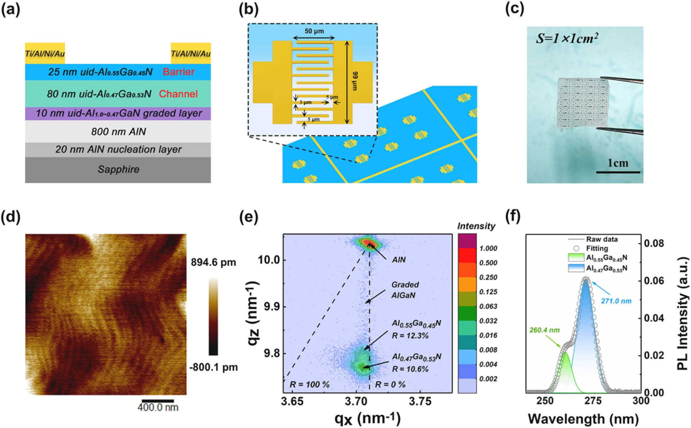
    Fig. 1. (a) Cross-sectional diagram of a phototransistor with ohmic-contact electrodes. (b) Configuration diagram of a planar phototransistor with interdigital electrodes. (c) Photograph of the planar interdigital electrode phototransistors on a chip with an area of 1  cm×1  cm. (d) AFM topography of sample surface with scanning area of 2  μm×2  μm. (e) XRD RSM of the sample recorded around (101¯5) reflection. The calculated full relaxation (R=100%) and full strain (R=0%) lines are also shown. (f) Room-temperature PL spectrum measured using a 213-nm laser as the excitation source.
    (a) Simulated energy band diagram of the phototransistor under zero bias voltage in the dark and 240 nm illumination of 0.1 μW/cm2 (upper panel) and the corresponding charge contributions (lower panel). (b) Directions of the spontaneous and piezoelectric polarization in our compressively strained Al0.55Ga0.45N/Al0.47Ga0.53N/AlN heterostructure. (c) Polarization charge distribution in the epitaxial structure under dark condition. (d) Comparison of the electric field distribution before and after 240-nm DUV illumination. (e) Cross-sectional view of the electron concentration distribution in the phototransistor before (left) and after (right) 240-nm DUV illumination.
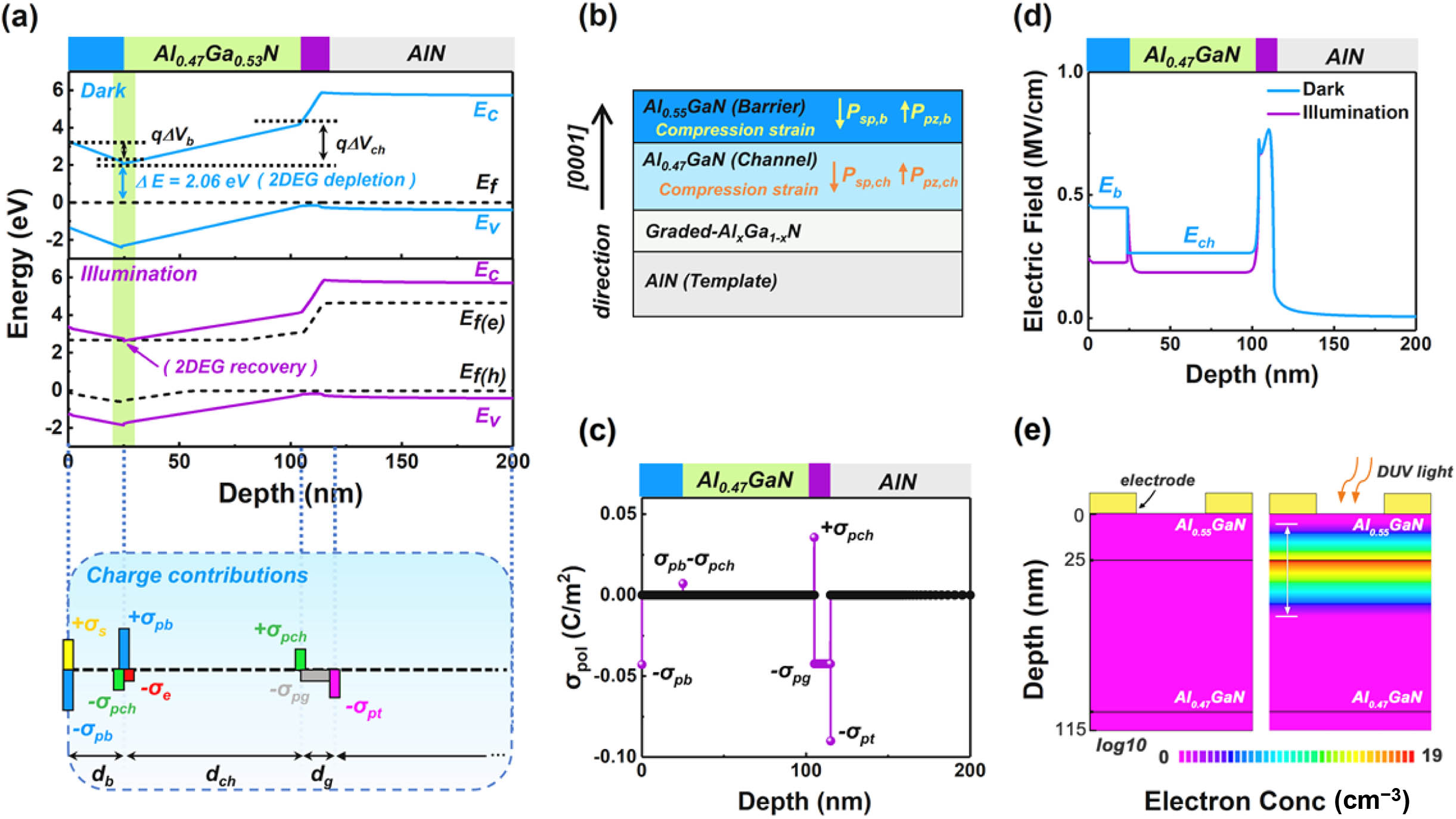
    Fig. 2. (a) Simulated energy band diagram of the phototransistor under zero bias voltage in the dark and 240 nm illumination of 0.1  μW/cm2 (upper panel) and the corresponding charge contributions (lower panel). (b) Directions of the spontaneous and piezoelectric polarization in our compressively strained Al0.55Ga0.45N/Al0.47Ga0.53N/AlN heterostructure. (c) Polarization charge distribution in the epitaxial structure under dark condition. (d) Comparison of the electric field distribution before and after 240-nm DUV illumination. (e) Cross-sectional view of the electron concentration distribution in the phototransistor before (left) and after (right) 240-nm DUV illumination.
    (a) C-V curves measured under the dark and the DUV illumination. (b) Depth profile of the apparent carrier density under the DUV illumination.
    Fig. 3. (a) C-V curves measured under the dark and the DUV illumination. (b) Depth profile of the apparent carrier density under the DUV illumination.
    Photoresponse characteristics of the phototransistor. (a) I-V curves under the dark and DUV illumination conditions. (b) Spectral response of the phototransistor under different bias voltages. (c) Time dependence of the response current to the 10 s/10 s on/off cycle incident DUV light with a time span of 80 days. (d) Transient response of the phototransistor to the 213-nm periodic pulse signals at 8 V. A magnified view of one of the impulse responses is shown in the inset. (e) Noise power spectral density measured at different bias voltages in the dark.
    Fig. 4. Photoresponse characteristics of the phototransistor. (a) I-V curves under the dark and DUV illumination conditions. (b) Spectral response of the phototransistor under different bias voltages. (c) Time dependence of the response current to the 10 s/10 s on/off cycle incident DUV light with a time span of 80 days. (d) Transient response of the phototransistor to the 213-nm periodic pulse signals at 8 V. A magnified view of one of the impulse responses is shown in the inset. (e) Noise power spectral density measured at different bias voltages in the dark.
    (a) Photograph of the measuring equipment for recording I-V-Pinc curves. (b) The I-V-Pinc curves of the phototransistor at the semi-logarithmic scale. (c) The linear scales at a DUV incident light power ranging from 0.6 fW to 6.7 nW. Pinc dependence of (d) the Iph and the PDCR and (e) D* at 10 V bias. (f) The theoretical Iph under the combination of photogating effects in the barrier and the channel layers. Schematic diagram of the energy band in the phototransistor under (g) dark, (h) low power irradiation, and (i) high power irradiation conditions.
    Fig. 5. (a) Photograph of the measuring equipment for recording I-V-Pinc curves. (b) The I-V-Pinc curves of the phototransistor at the semi-logarithmic scale. (c) The linear scales at a DUV incident light power ranging from 0.6 fW to 6.7 nW. Pinc dependence of (d) the Iph and the PDCR and (e) D* at 10 V bias. (f) The theoretical Iph under the combination of photogating effects in the barrier and the channel layers. Schematic diagram of the energy band in the phototransistor under (g) dark, (h) low power irradiation, and (i) high power irradiation conditions.
    SymbolDefinition
    σsCharges per unit area on the top surface
    σpbPsp and Ppz charges per unit area in the Al0.55Ga0.45N barrier
    σpchPsp and Ppz charges per unit area in the Al0.47Ga0.53N channel
    σeElectrons per unit area at the barrier/channel interface
    σpgPsp and Ppz charges per unit area in the graded AlxGa1xN region with layer thickness dg
    σptPsp and Ppz charges per unit area in the AlN template layer
    Table 1. Definition of Symbols Used in Charge Contributions
    Jiabing Lu, Zesheng Lv, Hao Jiang. AlGaN solar-blind phototransistor capable of directly detecting sub-fW signals: self-depletion and photorecovery of full-channel 2DEG enabled by a quasi-pseudomorphic structure[J]. Photonics Research, 2023, 11(7): 1217
    Download Citation