Heterojunction field-effect phototransistors using two-dimensional electron gas (2DEG) for carrier transport have great potential in photodetection owing to its large internal gain. A vital factor in this device architecture is the depletion and recovery of the 2DEG under darkness and illumination. This is usually achieved by adding an external gate, which not only increases the complexity of the fabrication and the electrical connection but also has difficulty ensuring low dark current (). Herein, a quasi-pseudomorphic AlGaN heterostructure is proposed to realize the self-depletion and photorecovery of the 2DEG, in which both the barrier and the channel layers are compressively strained, making the piezoelectric and spontaneous polarization reverse, thus depleting the 2DEG and tilting the entire barrier and channel band to form two built-in photogates. The fabricated solar-blind phototransistors exhibit a very low below , a superhigh responsivity () of , a record high detectivity () of Jones, and an ultrafast response speed at the nanosecond level. The high performance is attributed to the efficient depletion and recovery of the full 2DEG channel by the two photogates, enabling direct detection of the sub-fW signal. This work provides a simple, effective, and easily integrated architecture for carrier control and supersensitive photodetection based on polarization semiconductors.
1. INTRODUCTION
Photodetection in the solar-blind deep ultraviolet (DUV) wavelength region is of central importance in various civil and industrial applications [1]. Recently, the research of solid-state semiconductor DUV photodetectors has attracted much attention, stimulated by the development needs of its small size, energy-saving, and smart detection modules [2,3]. For solar-blind DUV detection, however, sensitivity below the magnitude of fW is generally required in many key applications, including flame sensing [4], corona discharge observations [5], UV astronomy [6], and biological and chemical agent detection [7]. Although this demand is in line with the current development trend of single-photon detection, it poses a very challenging task for the signal response capability of solid-state DUV detectors. The photocurrent (), a general response signal, depends on the number of carriers flowing through the electrode area per unit time under illumination. Therefore, the number of carriers and the transit time under the incident light are two fundamental factors needed to improve the photoresponse performance.
Not only the number of carriers but also the transport time can be controlled by the nanoscale low-dimensional material structure. As a representative form of carrier existence and transport in a low-dimensional structure, two-dimensional electron gas (2DEG) has many critical applications in high-gain and high-speed heterojunction field-effect transistors (FETs)/phototransistors (FEPTs) due to its inherent characteristics of high electron density and high mobility [8–11]. The FEPTs with a 2DEG based on GaAs, InP, and GaN material systems have demonstrated highly sensitive detection performance in the terahertz, infrared, and UV bands [12–14]. A prominent problem affecting the performance of such structured phototransistors is the low signal-to-noise ratio and inferior sensitivity caused by the 2DEG existing in both dark and illumination conditions. To settle this problem, research efforts are usually from the perspective of the device structure, namely introducing a Schottky barrier or a PN junction gate to deplete the 2DEG in the channel below, rather than looking for solutions from the perspective of material properties [12–16]. Such a solution, however, suffers from the increased complexity of the device fabrication and the electrical connection. Second, it is difficult to ensure very low dark current () only by depleting a small part of the 2DEG channel below the gate, which is particularly critical for the weak light detection of the photodetector. Lastly, the incidence of the optical signal from different sides of the gate will lead to the different directions of the 2DEG channel current, which may cause the offset of the signal current and may cause the burden on the signal processing circuit [17].
Spontaneous polarization (), caused by the non-coincidence of the positive and negative charge centers in the lattice equilibrium, exists widely in non-centrosymmetric compound semiconductors, such as the wide band gap (WBG) compound semiconductors (Al)GaN, ZnO, and [18–21]. Moreover, when the semiconductor is strained, the lattice deformation induces a further separation of the centers of positive and negative charges in the crystal, thus forming dipole moments, whose accumulation leads to the polarization charges on the crystal surface. This additional polarization due to the strain is named piezoelectric polarization (). In the heterostructure of the polarization semiconductors, even under the condition of unintentional doping, high-density 2DEG with high mobility can be generated at the heterointerface due to the presence of a polarization-induced sheet charges on the bottom and top surfaces of the barrier layer [22–24].
Sign up for Photonics Research TOC. Get the latest issue of Photonics Research delivered right to you!Sign up now
Compared with other WBG materials, AlGaN with a direct and tunable bandgap has gone from exploratory research to industrial application [25,26], but like other WBG materials, its solar-blind UV photodetection applications are still under exploration [27]. For the -plane wurtzite AlGaN heterojunction, the barrier layer is generally grown on the relaxed channel layer where the occurs along the [0001] direction, and the in the barrier is in the same direction as the , which enhances the total polarization and leads to strong electric fields of MV/cm magnitude along the growth axis and polarization-bound charges with a sheet density of or higher at the barrier/channel interface. The positive bound sheet charge at the upper barrier/channel interface induces the accumulation of electrons at the lower interface, thus forming high-density 2DEG without intentional doping. Benefiting from this characteristic advantage, in addition to the FETs, the AlGaN heterojunction has also recently gained much attention in building the UV FEPTs. Previous research has shown the strong capability of such UV FEPT to achieve a high responsivity (), a high rejection ratio, and a high detectivity (). Two-terminal AlGaN/GaN heterojunction FEPTs have been realized by introducing a p-GaN floating junction gate to deplete the 2DEG channel under dark conditions [28–30]. This structured visible-blind UV detector exhibited high performance with an up to and a response time as fast as 11.33 μs/65.52 μs. By replacing the gate with negatively biased semitransparent Schottky contacts [31,32], the three-terminal AlGaN/GaN heterojunction FEPTs achieved a high of and an ultra-high specific of Jones. Several groups tried to suppress by recess-etching 2DEG channels [33,34]. With this configuration, a photo-to-dark current ratio (PDCR) of can be obtained at the cost of reducing the response to or less. Efforts have also been devoted to developing solar-blind Al-rich AlGaN heterojunction FEPTs. Despite the influence of the poor crystalline quality of Al-rich AlGaN and the shading effect of the gate, the AlGaN solar-blind phototransistors with a Ni/Au Schottky gate still demonstrate an of up to [35]. Floating p-GaN and p-AlGaN junction photogates have also been employed in the AlGaN solar-blind FEPTs, respectively [36,37]. Due to avoiding the absorption of the p-GaN to the incident DUV signal, the AlGaN heterojunction FEPTs with the p- junction gate achieved a high of , an extremely high PDCR of , and the consequently ultrahigh of Jones, showing the great potential for detecting weak signals [37]. Although these works have brought significant progress to AlGaN solar-blind UV FEPTs, the improvement approaches basically follow the method of controlling the 2DEG channel in heterojunction electronic devices.
In this work, the intrinsic piezoelectric polarization is used to realize the self-depletion and photorecovery of full-channel 2DEG through a quasi-pseudo AlGaN heterostructure. With such a heteroepitaxial structure, the barrier and channel AlGaN layers are both compressively strained, resulting in the in the barrier opposite the , thus prompting the depletion of the full 2DEG channel. Meanwhile, the polarization induces the built-in longitudinal electric fields through the barrier and the channel layers, respectively, which acts as the photogates to restore the full channel 2DEG under the incidence of the DUV signal. The self-depletion of the 2DEG and the recovery under the double photogates brought dramatic improvements in the , specifically in , reaching and Jones, respectively, which are more than two orders of magnitude of the previous record. These excellent performances enable the detector to directly detect sub-fW DUV signals.
2. MATERIALS AND METHODS
A. Material Epitaxy
The wafer sample was epitaxially grown on a -plane sapphire substrate using the metal-organic chemical vapor deposition (MOCVD) method. Ammonia (), trimethylgallium (TMGa), and trimethylaluminum (TMAl) were used as the precursors for N, Ga, and Al, respectively, and hydrogen () was used as the carrier gas. The epitaxy started with the annealing of the substrate at 1090°C under for 5 min. Subsequently, a 20-nm-thick AlN nucleation layer was deposited at 780°C. After that, the growth temperature was ramped to 1080°C. An 800-nm-thick unintentionally doped (uid) AlN back barrier layer was deposited by the pulsed growth method, in which was introduced into the reactor with 6 s on and 12 s off while TMAl was always on. Next, a 10-nm-thick compositionally graded uid- () buffer layer, an 80-nm-thick uid- channel layer, and a 25-nm-thick uid- front barrier layer were deposited sequentially.
B. Device Fabrication
The phototransistor was fabricated by using a simple non-etching planar process. Prior to device fabrication, the wafer sample was individually cleaned with acetone, isoproponal (IPA), and deionized (DI) water for 10 min and immersed in a HCl:DI water (1:1) solution for 10 min to remove the surface oxide. Then, the electrode pattern was formed by standard photolithography. Next, Ti/Al/Ni/Au (15 nm/80 nm/20 nm/60 nm) interdigital electrodes were directly deposited on the clean wafer surface by electron beam evaporation and thermal evaporation, followed by rapid annealing at 830°C in a high-purity atmosphere for 30 s to form ohmic contacts. The interdigital electrodes are composed of 13 electrode fingers, of which the length, width, and spacing of the interdigital electrodes are 45 μm, 3 μm, and 5 μm, respectively. The effective absorption area is therefore μ.
The Schottky barrier diodes used for the capacitance-voltage (C-V) measurements were fabricated on the same chip as the phototransistor. The circular Schottky contacts were formed by depositing Ni/Au metal bilayers with a thickness of 20 nm/100 nm and a 200 μm diameter. Ti/Al/Ni/Au (15 nm/80 nm/20 nm/60 nm) metal stacks were deposited by e-beam evaporation and thermal evaporation on the wafer surface and subsequently annealed at 830°C for 30 s to form annular ohmic contacts.
C. Characterization
Structural properties of the epitaxial sample were characterized by high-resolution X-ray diffraction reciprocal space mapping (XRD-RSM) measurements (Brucker D8 Discovery). The surface morphology of the epitaxial structure was characterized by an atomic force microscope (AFM) tapping mode (Brucker Dimension Edge). The room-temperature photoluminescence (PL) spectrum was obtained through a spectrometer (Nanometerics RPMBlue) with a 213-nm excitation pulse laser. For device performance characterization, dark and illuminated current-voltage (I-V) and C-V curves were measured using a semiconductor parameter analyzer (Keithley SCS-4200). A light emitting diode (LED) with a central wavelength of 260 nm was used as the excitation source for the top illumination. The LED is coupled to an optical fiber with a spot diameter of 5 mm on the photodetector. The incident optical power density was calibrated by an optical power meter (Newport 843-R). In the measurements, except for the test of changing the incident power, the incident optical power density is fixed at μ. The spectral responses were recorded with a test platform equipped with a 1200 gr/mm grating monochromator and a combined light source consisting of a deuterium lamp and a tungsten bromide lamp coupled to a fiber with a 2-mm-diameter spot. Transient responses were measured using a 213-nm DUV laser as an excitation source (Brolight MCC-213-1004) with a pulse width of 700 ps and a repetition frequency of 1 kHz, while the response signal was recorded by a high-speed oscilloscope (Keysight DSOS604A). Noise power spectral density was collected by a noise measurement system (PDA FS-Pro, 100 kHz bandwidth).
3. RESULTS AND DISCUSSION
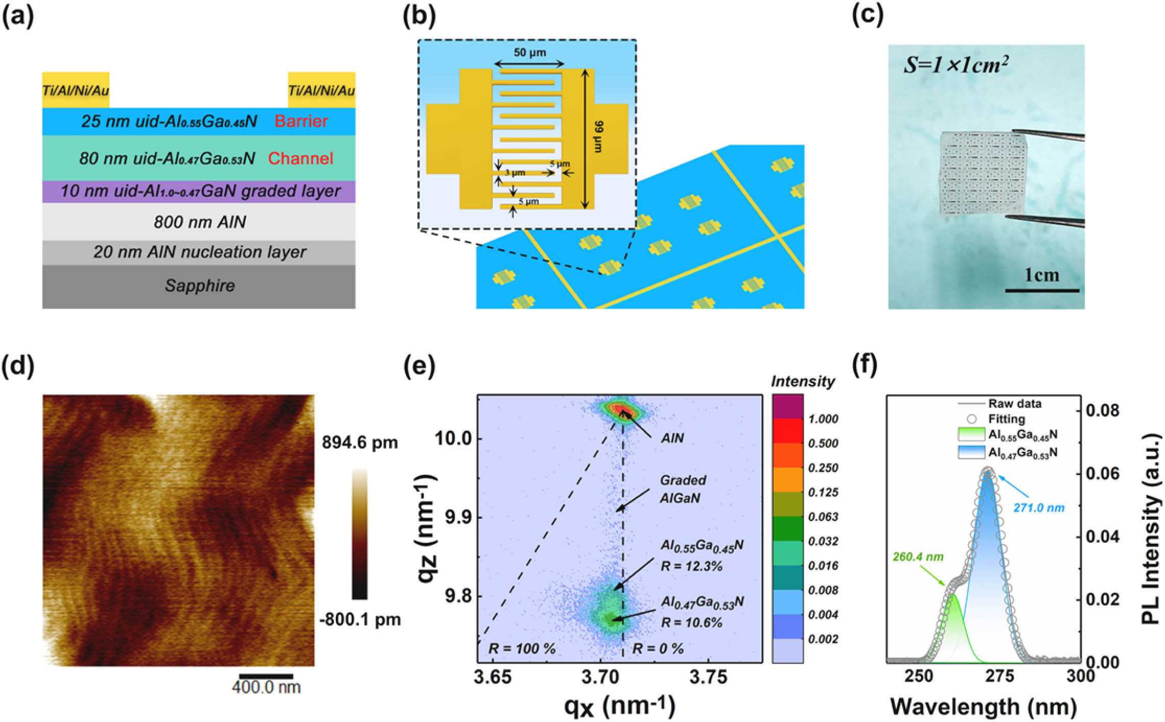
Figure 1(a) shows a schematic cross section of the device structure. The structure is composed of quasi-pseudomorphic epilayers. This was accomplished by using a relatively thin AlGaN channel layer together with a thin graded layer to suppress strain relaxation. Referring to the strain-relaxation critical thickness of the epilayer on the AlN [38], we chose a total thickness of 105 nm for the barrier and channel layers to achieve quasi-pseudomorphic epitaxy. Figures 1(b) and 1(c) exhibit the electrode configuration and chip photograph of the resulting planar phototransistors. Before the device processing, the as-grown epitaxial structure was characterized by AFM, XRD-RSM, and PL measurements. As shown in Fig. 1(d), the AFM morphology indicates that the sample is deposited by the step-flow growth mode and has a smooth surface with a root-mean-square roughness of 0.21 nm.
Figure 1.(a) Cross-sectional diagram of a phototransistor with ohmic-contact electrodes. (b) Configuration diagram of a planar phototransistor with interdigital electrodes. (c) Photograph of the planar interdigital electrode phototransistors on a chip with an area of . (d) AFM topography of sample surface with scanning area of μμ. (e) XRD RSM of the sample recorded around () reflection. The calculated full relaxation () and full strain () lines are also shown. (f) Room-temperature PL spectrum measured using a 213-nm laser as the excitation source.
From the RSM around the asymmetric () reflection [Fig. 1(e)], it is found that the (, ) coordinates of the reciprocal lattice points (RLPs) of the AlGaN barrier are (3.705, 9.806), while those of the AlGaN channel are (3.705, 9.769). Both the front barrier and the channel layer are quasi-pseudomorphic to the underlying AlN back barrier with the (, ) coordinates of (3.710, 10.037). The in-plane and out-of-plane lattice parameters, and , of the AlGaN layers can be calculated from the coordinates of the asymmetric ()-plane RLP using and . Consequently, the in-plane lattice constants of the barrier and the channel are 0.3117 nm, while that of the AlN template layer is 0.3112 nm. Using the method reported by Pereiea et al. [39], the Al composition of the barrier and the channel layers estimated from the measured lattice constants is 55% and 47%, respectively. The lattice constants corresponding to the strain-free barrier, the channel, and the AlN layers are 0.3155, 0.3149, and 0.3112 nm, respectively, indicating that the barrier and channel layers are both compressively strained. The relaxation degree of the barrier and the channel relative to the AlN layer is 12.3% and 10.6%, respectively. As discussed later, the strong compressive strain (small relaxation) of the AlGaN barrier and the channel layers is the key factor for the self-depletion of the 2DEG channel and the enhancement of the photogating effect. Finally, the PL spectrum of the wafer samples was measured to characterize its optical properties [Fig. 1(f)]. The main emission peak centered at 271.0 nm (blue curve) is assigned to the channel, while the short wavelength shoulder peak at 260.4 nm (green curve) is attributed to the barrier, which is consistent with the Al compositions of the barrier and the channel layers obtained by the RSM.
Figure 2.(a) Simulated energy band diagram of the phototransistor under zero bias voltage in the dark and 240 nm illumination of μ (upper panel) and the corresponding charge contributions (lower panel). (b) Directions of the spontaneous and piezoelectric polarization in our compressively strained heterostructure. (c) Polarization charge distribution in the epitaxial structure under dark condition. (d) Comparison of the electric field distribution before and after 240-nm DUV illumination. (e) Cross-sectional view of the electron concentration distribution in the phototransistor before (left) and after (right) 240-nm DUV illumination.
In general, because of equilibrium, the entire heterostructure needs to have an overall charge neutrality and a zero external electric field [41]. Applying Gauss’s law at the barrier/channel interface as indicated in Fig. 2 gives εσσσwhere and are the permittivities of the channel and barrier, and and are the electric fields in the channel and barrier. Equation (1) can be further expressed in the form that each term is a sheet charge density (satisfying charge neutrality) as σwhere is the residual barrier polarization left by the neutralizing effect of the surface charges (i.e., ), and is the residual channel polarization after neutralization of the surface charges by the channel polarization and the interfacial electron. and are the voltage drops on the barrier and the channel, and and are the barrier and the channel thicknesses. Figure 1 shows that the key to eliminating the 2DEG in the equilibrium state is to reduce the (barrier polarization) or increase the (channel polarization). In the polarization consisting of and , the strain-dependent has a large adjustable degree. The pseudomorphic or quasi-pseudomorphic epilayer structure, however, can regulate to eliminate the 2DEG at the barrier/channel interface in the equilibrium state. In the case of such a heterostructure, the barrier layer is compressively strained, which makes the partially offset by in the opposite direction [Fig. 2(b)], thus reducing or even making . In the usual barrier/channel heterostructure, however, the barrier layer is tensile-stressed, where the and are in the same direction, which increases . The surface density of charges () oriented along the -axis of the wurtzite AlGaN layer is related to the Al composition , namely , while the surface density of charges can be determined by using the lattice constants and basal strain of the AlGaN epitaxial layer [40,42]. Figure 2(c) gives the resulting sheet polarization charge density () at each interface of the heterostructure, including and . The energy band diagram of the quasi-pseudomorphic heterostructure is thus simulated [the upper panel of Fig. 2(a)], from which the voltage drops and are 1.21 V and 2.42 V, respectively. We then obtained at the lower interface of the barrier/channel by using Eq. (2), which corresponds to a sheet electron density () of about . All these suggest that the quasi-pseudomorphic heterostructure can regulate the polarization effects to effectively eliminate the 2DEG. In addition, as shown in Fig. 2(d), the built-in electric fields () in the barrier and () in the channel are 0.45 MV/cm and 0.26 MV/cm, respectively in the equilibrium state, which can effectively separate photogenerated electron hole pairs (EHPs).
Upon 240-nm DUV illumination, the energy band tilt of both the barrier and the channel layers decreases, and the channel 2DEG recovers [the middle in Fig. 2(a)]. This recovery is due to the fact that the built-in electric fields are partially offset by the separation of the photogenerated EHPs. The photogenerated EHPs are separated and swept toward the different interfaces by the built-in electric fields, making the electron/hole quasi-Fermi energy levels separate. Among them, the photoelectrons in the barrier and channel layers move toward the barrier/channel heterointerface, contributing to the recovery of the 2DEG, while the photoholes move toward the surface and the graded uid-, respectively, and accumulate there. The overall distribution of the electric field in Fig. 2(d) shows that under DUV illumination, the and in the barrier layer and the channel layer are significantly lower than those in the dark. That is, the photovoltage () generated by the EHP separation in the barrier (channel) layer lowers the voltage drop on the layer, which is equivalent to applying a positive bias on the virtual gate in the layer. Figure 2(e) gives the electron concentration distribution in the active layers of the photodetector before and after the 240-nm DUV illumination. In the dark, there are no electrons in the active layers, while the electrons under the DUV illumination are distributed with the maximum density at the quasi-triangular potential well of the barrier/channel heterointerface. The maximum electron concentration under the μ illumination is . These simulations show that the 2DEG channel can be depleted by making the in the barrier opposite to the and can be recovered by light absorption of the barrier and the channel layers. The concentration of the recovered 2DEG, however, depends on the incident DUV light intensity.
The recovery effect of the incident light on the 2DEG channel was first confirmed by measuring the C-V under dark and DUV illumination. Planar Schottky diodes were fabricated on the same wafer sample as the phototransistor to measure the C-V characteristics. Figure 3(a) shows the C-V curves obtained at a 10 kHz test frequency. The inset gives the top view microscope image of the Schottky diodes with an active area diameter of 200 μm. One can see that the dark capacitance () shows a constant low value of about 140 fF in the reverse bias range of 0–10 V, indicating that there are only a few electrons in the channel, that is, the channel is fully depleted by the built-in polarization-induced photogate and is in the off state. Under the 260-nm illumination with an intensity of μ, the photo-capacitance () rises from about and reaches a saturation value of at a bias voltage between and 0 V. The apparent carrier concentration under the illumination as a function of depth can be calculated by the following Eqs. (3) and (4) [43]: where , , , , and are the electronic charge, the dielectric constant, the vacuum dielectric constant, the Schottky contact area, and the applied voltage, respectively. The depth profile shown in Fig. 3(b) demonstrates that the peak is from the surface, indicating that there is a 2DEG confined to the lower interface under the illumination. Furthermore, the sheet carrier concentration in the channel can be obtained by [43]. The resulting value of the 2DEG channel recovered by the DUV light is . This shows that in the off state the channel can normally change to the on state due to the light recovery of the 2DEG.
Figure 3.(a) C-V curves measured under the dark and the DUV illumination. (b) Depth profile of the apparent carrier density under the DUV illumination.
We then fabricated the phototransistors and characterized their solar-blind photodetection performance. Figure 4(a) exhibits the typical I-V characteristics of the phototransistors measured in the dark and illumination conditions. At 10 V bias, the is only 0.5 pA, corresponding to the dark current density calculated by taking the total length of the interdigital electrodes as the effective gate width. We attribute the very low to the efficient depletion of the 2DEG brought about by manipulating the in the barrier layer through the quasi-pseudomorphic heterostructure. Under μ top illumination with a wavelength of 260 nm, the photocurrent density measured at 10 V is as high as 0.8 mA/mm. Consequently, an extremely high PDCR of was obtained, benefiting from a low and a high gain.
Figure 4.Photoresponse characteristics of the phototransistor. (a) I-V curves under the dark and DUV illumination conditions. (b) Spectral response of the phototransistor under different bias voltages. (c) Time dependence of the response current to the 10 s/10 s on/off cycle incident DUV light with a time span of 80 days. (d) Transient response of the phototransistor to the 213-nm periodic pulse signals at 8 V. A magnified view of one of the impulse responses is shown in the inset. (e) Noise power spectral density measured at different bias voltages in the dark.
We further performed spectral response measurements of the phototransistor using an optoelectronic test platform, as shown in Fig. 4(b). The spectral responsivity is obtained according to Eq. (5), where is the incident light power density at wavelength , and is the total device absorption area. The photodetector clearly shows a solar-blind cutoff wavelength at , which is consistent with the absorption edge of the channel layer. At 3 V bias, the peak responsivity, , at 260 nm is as high as . Since the band edge of the barrier layer is at 260 nm [Fig. 1(f)], this peak position indicates that the is not only contributed by the photogenerated carriers in the channel layer but also by those from the barrier layer. The increases with the bias voltage, which is mainly due to the increase of transconductance with the bias.
The dynamic photodetection performance of the phototransistors was investigated by continuously modulating the incident light. Figure 4(c) shows the time dependence of the response current of the phototransistor to the incident DUV light of the periodic switch at the 8 V bias. The detector presents a repeatable and stable response current to the incident DUV light with an on/off period of 10 s. Moreover, even after being stored in air for 80 days, it still shows the same stable time dependence. Since the maximum speed of the electronic shutter used for the incident light modulation is 0.3 s, the response time cannot be accurately derived from the rising and falling edges of the response current. Therefore, the transient response was assessed by a 213-nm pulsed laser excitation, a 50-Ω load resistor, and a high-speed oscilloscope. Three typical impulse responses are captured in Fig. 4(d). From the single impulse response curve [the inset of Fig. 4(d)], it can be determined that the rise time from 10% to 90% of the response peak is 620.7 ps, while the decay time from 90% to 10% of the peak is 123.5 ns. The rise time is approximately equal to the electron transit time () between the positive and negative electrodes. The relatively long decay time, however, is probably due to the release of trapped minority carrier holes from deep-level defects after the pulsed light.
The noise power spectral density () was measured at room temperature at 3 V, 5 V, and 10 V bias. As shown in Fig. 4(e), the is inversely proportional to the frequency in the range of 1 Hz to 1 kHz, indicating that flicker () noise dominates under this condition. In addition, the increases with the bias voltage. At frequencies above 1 kHz, however, the of the phototransistor is maintained at a level of due to the limitations of the measurement equipment.
To further clarify the operating mechanism of this phototransistor, we analyzed the dependence of the I-V curve on the incident light power (). The measuring equipment used to record the curves is shown in Fig. 5(a), with an optical attenuator introduced to change the incident light intensity. Figures 5(b) and 5(c) present the I-V curves in the range of the incident DUV light intensity from to (corresponding to the from 0.6 fW to 6.7 nW) in logarithmic and linear coordinates, respectively. At extremely weak incident power below 10 fW, the gradually rises with the increase of bias voltage and then tends to saturation. Such lower at a low bias voltage is attributed to the trapping of photogenerated carriers by deep level defects in the barrier and channel layers, which weakens the contribution of photogenerated carriers to the virtual gates in these two layers and leads to low 2DEG density. With the increasing bias voltage, the increases gradually due to the increase of the drift velocity of the 2DEG channel. Further increasing the bias, the tends to be saturated due to the drain (anode) pinch-off. In contrast, at an irradiation power above 10 fW, the increases rapidly with the increasing bias voltage. As shown in Fig. 5(c), the curves of the photodetector present the typical output characteristics of the FETs, which can be divided into three regions, namely, the linear region, the nonlinear region, and the saturation region. Since increasing the is equivalent to applying a positive bias voltage to the virtual gates, the (drain current) increases with the . At a bias voltage of 10 V, the rapidly increases linearly with the and then becomes saturated, showing excellent transfer characteristics (drain current versus gate voltage) of FETs [Fig. 5(d)].
Figure 5.(a) Photograph of the measuring equipment for recording curves. (b) The curves of the phototransistor at the semi-logarithmic scale. (c) The linear scales at a DUV incident light power ranging from 0.6 fW to 6.7 nW. dependence of (d) the and the PDCR and (e) at 10 V bias. (f) The theoretical under the combination of photogating effects in the barrier and the channel layers. Schematic diagram of the energy band in the phototransistor under (g) dark, (h) low power irradiation, and (i) high power irradiation conditions.
The specific detectivity (), a crucial figure of merit for the DUV photodetector, can be calculated according to the noise equivalent power (NEP) using the following formulas [44], where is the electrical bandwidth and is the total noise current power. By integrating the in Fig. 4(e) [i.e., ], the is estimated to be . The can then be obtained at the test bandwidth . Figure 5(e) shows the as a function of the incident light power at a bias voltage of 10 V. A maximum of Jones was calculated with at an optical power of 0.6 fW, demonstrating the extremely weak signal sensing capability of such photodetectors in the solar-blind band. Moreover, the decreases with the increase of , which is due to the fact that the tends to saturate with the (the photogating effect tends to saturate) [45].
To further explain the reason behind the high sensitivity response, we performed the analysis by building an model. Under the DUV illumination, the increase in the channel current, , originates from the photogating effect of the virtual gates in the barrier and channel layers. Thus, the can be expressed as where and are the transconductances of the barrier layer and the channel layer, and and are corresponding photovoltages, respectively. The transconductance can be given by [46] where is the finger length of the interdigital electrode, is the electron mobility, and is the finger spacing. The capacitance is the capacitance per unit area between the 2DEG channel and the barrier layer () or the channel layer (), which can be simplified as , where is the dielectric constant of the channel or barrier, and is the barrier or channel thickness. It was calculated that the and of the phototransistor are and , respectively. One can see from Eq. (9) that the benefits from the mobility of the 2DEG, the adjustable spacing and length of the interdigital electrodes, and the thickness of the thin barrier and channel layers.
The photovoltage can be considered a function of the concentration of the photoexcited holes accumulated at the surface or at the back of the heterointerface, which can be expressed as where is the effective density of states in the valence band and is defined as , where is the effective hole mass, and is the Planck constant. The hole effective mass, , of () and () is obtained by linear interpolation of the AlN and GaN values [47]. The values of the barrier layer and channel layer are calculated as and , respectively. In addition, the is defined as the number of photogenerated holes per unit volume within the minority carrier lifetime , namely , where is the energy of the incident photon. Using the absorption coefficient [48], thickness, and reflectivity of the barrier layer and the channel layer at 260 nm, the external quantum efficiency and values of the photogenerated carriers are estimated to be 0.22 and 0.41, respectively. As a result, the , PDCR, and , calculated from the model described above, are shown by the solid lines in Figs. 5(d) and 5(e). These theoretical values are in good agreement with the measurements, confirming that the main mechanism of the high sensitivity of our phototransistor is the photogating effect of generating positive photovoltages to the polarization built-in virtual photogates. Figure 5(f) shows the and , calculated by the model which originate from the barrier and the channel layers, respectively, indicating that the photogating effect in the channel layer is the main contributor to the . At 10 V bias and , the estimated values of and are 0.13 mA/mm and 0.68 mA/mm, respectively. Figures 5(g)–5(i) show the energy band diagrams of the phototransistor under non-irradiation, lower power irradiation, and higher power irradiation. With the increase of , the photogenerated EHPs in the barrier and the channel layers are separated under the action of the polarization fields, which makes the 2DEG channel and the holes accumulated on the surface and at the back heterointerface increase. The resulting and reduce the energy band tilt of the barrier layer and the channel layer, and widen the 2DEG channel, thus increasing the .
4. CONCLUSIONS
In conclusion, we have developed a novel heterojunction FEPT capable of directly detecting sub-fW signals. A quasi-pseudomorphic heterostructure was utilized to manipulate the piezoelectric polarization effect, where both the barrier and channel layers are subjected to compressive strain, causing opposite and thus 2DEG depletion, while a built-in electric field (energy band tilt) is introduced throughout the barrier and channel layers. As a result, the self-depletion and photorecovery of the full-channel 2DEG are achieved. The resulting phototransistor exhibits a superhigh performance, including a very low , a high PDCR (), a large (), a record specific ( Jones), and a high response speed with rise/fall time of 620.7 ps/123.5 ns. The low is attributed to the effective depletion of the full channel, while the large is ascribed to the large internal gain due to the photogating effect. The internal gain depending on the transconductance and the photovoltage, however, benefits from the 2DEG mobility, the spacing and finger length of the interdigital electrodes, and the thickness of the thin barrier and channel. We believe the detection performance can be further improved by optimizing the above factors. Our work provides a simple and easily integrated way to realize carrier regulation and supersensitive detection based on polarization compound semiconductors.