Shi Zhao, Li Lizhu, Zhao Yu, Fu Ruxing, Sheng Xing. Implantable Optoelectronic Devices and Systems for Biomedical Application[J]. Chinese Journal of Lasers, 2018, 45(2): 207001
Search by keywords or author
- Chinese Journal of Lasers
- Vol. 45, Issue 2, 207001 (2018)
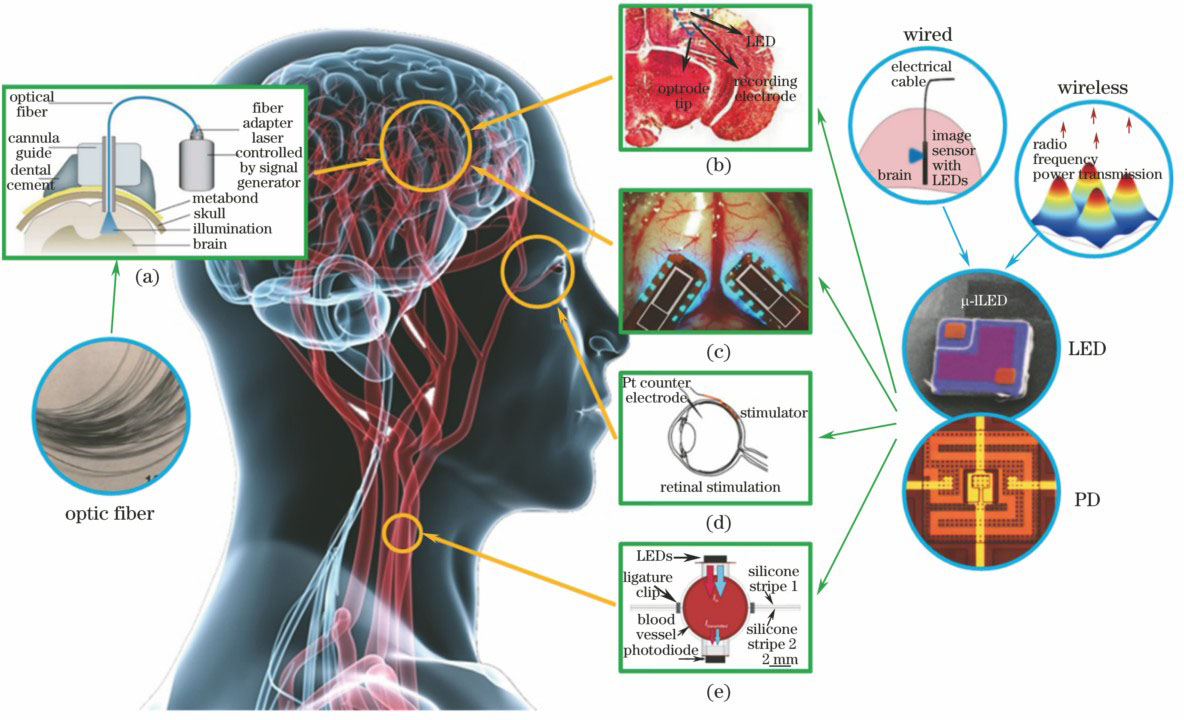
![Application schematic of implantable optoelectronic devices (a) Optogenetics with optical fiber[13]; (b) optogenetics probe[14]; (c) intracranial fluorescence imaging device[15]; (d) retinal prosthesis stimulator[16]; (e) extravascular oxygen monitor[17]](/richHtml/zgjg/2018/45/2/0207001/img_1.jpg)
Fig. 1. Application schematic of implantable optoelectronic devices (a) Optogenetics with optical fiber[13]; (b) optogenetics probe[14]; (c) intracranial fluorescence imaging device[15]; (d) retinal prosthesis stimulator[16]; (e) extravascular oxygen monitor[17]
![Biomedical applications of silica fibers and multifunctional flexible polymer fibers. (a) Silica fibers for optogenetics experiments[22]; (b) mouse brain implanted with silica fibers[23]; (c) schematic of fiber implanted in specific brain sections for biological fluorescence photometry[26]; (d) biological fluorescence photometry system[26]; (e) fabrication of preforms[30]; (f) thermal drawing process[32]; (g) cross section of fiber[30]; (h) fiber probe implanted into mouse brain[30]; (i) electro](/richHtml/zgjg/2018/45/2/0207001/img_2.jpg)
Fig. 2. Biomedical applications of silica fibers and multifunctional flexible polymer fibers. (a) Silica fibers for optogenetics experiments[22]; (b) mouse brain implanted with silica fibers[23]; (c) schematic of fiber implanted in specific brain sections for biological fluorescence photometry[26]; (d) biological fluorescence photometry system[26]; (e) fabrication of preforms[30]; (f) thermal drawing process[32]; (g) cross section of fiber[30]; (h) fiber probe implanted into mouse brain[30]; (i) electro
Fig. 3. Hydrogel optical waveguides and biodegradable optical devices. (a) Light-guiding hydrogel of encapsulating cells[33]; (b) optimizing waveguides by adjusting molar weights[33]; (c) schematic of comparing between light-scattering profiles at mouse back with (top) and without (bottom) hydrogel implant[33]; (d) fabrication steps of hydrogel fibers[34]; (e) hydrogel fibers with different core sizes[34]; (f) light guidance of hydrogel fiber in air (left) and porcine slices (right)[34]; (g) transparent
Fig. 4. Fabrication of thin films for optoelectronic devices. (a) Silicon thin film obtained by method of SOI stripping[46]; (b) schematic of steps for selective fabricating bulk quantities of silicon micro-nanoribbons in multilayer stacked Si(111) wafer[47]; (c) schematic of laser lifting off of GaN thin films from sapphire[48]; (d) anisotropic etching of silicon to fabricate GaN thin film[49]; (e) schematic of method for preparing gallium arsenide by using aluminum arsenide as sacrificial layer[52]; (
Fig. 5. Flexible interconnect andits applications in biology. (a) One-dimensional (left)[62] and two-dimensional (right)[63] "wave-shaped" silicon thin films; (b) flexible electronic structure with "bridge structure"[64]; (c) serpentine interconnect structure[65]; (d) raised islands arranged on elastic substrate[66-67]; (e) two-dimensional fractal layout of U-shaped serpentine curves[68]; (f) red LED array with serpentine metal bridges transfer printed on fingertip region of vinyl glove[69]; (g) hemisph
Fig. 6. Devices 1 for energy transmission. (a)(b) Microscopy system of biological brain imaging[3,80] with scale of 5 mm and 1 cm, respectively; (c)(d) miniaturized high-resolution two-photon brain imaging system[82]; (e) schematic of achieving optogenetics virus import by FUS[83]; (f)(g) schematic of devices using solar cells for power supply[89]; (h) structural diagram of fully degradable metal battery[90]; (i) schematic of working principle of new-type bio-battery[91]
Fig. 7. Devices 2 for energy transmission. (a) Schematic of working principle of thermoelectric device[94]; (b) schematic of working principle of piezoelectric device getting energy from heart[95]; (c) schematic of deformation of piezoelectric devices getting energy from skin[96]; (d) schematic of coil coupling device[97]; (e) structural diagram of capacitive coupling receiver[98]; (f) photograph of capacitive coupling device[98]; (g) schematic of device using solar cells for power supply[89]; (h) photo
Fig. 8. (a) Schematic of implantable optical sensor developed by Animas for blood glucose measurement based on near-infrared absorption spectrum[119]; (b) design block diagram of implantable near-infrared optical device for blood glucose measurement with high precision and high sensitivity[120]; (c) photograph of miniature electronic platform for long-term implantable fluorescent biosensor, implanted in animals, inset: structural diagram of implantable electronic platform[125]; (d) glucose reactive fluo
Fig. 9. (a) Photograph of implantable bio-luminescence detector using VCSEL as excitation source, inset: internal structure of fluorescence detector[148]; (b) photograph of implantable bio-luminescence detectors using CMOS ROIC, implanted in free-moving mouse, inset: internal structure and appearance of sensor[4]; (c) photograph of deep brain fluorescence imaging device using CMOS image sensor, implanted in hippocampus of mouse brain, inset: photograph of shank imaging device[151]; (d) method of brain e
Fig. 10. (a) Schematic of fiber guide system based on cannula guide in earlier optogenetics research[13]; (b) photograph of fiber-LED-coupled implantable optogenetics stimulator, with fiber implanted into mouse brain, inset: each part and overall structure of stimulator[161]; (c) schematic of nerve probe with integrated LED light source and microelectrode, implanted into brain tissue, inset: SEM of probe, scale of 400 μm[14]; (d) microscope image of complex neuro-probe by combining electrical recording a
|
Table 1. Summary of transmission modes for energy and information

Set citation alerts for the article
Please enter your email address


