
Xiaoshu Guo, Sandong Guo. Janus MSiGeN4 (M = Zr and Hf) monolayers derived from centrosymmetric β-MA2Z4: A first-principles study[J]. Journal of Semiconductors, 2021, 42(12): 122002
- Journal of Semiconductors
- Vol. 42, Issue 12, 122002 (2021)
Abstract
1. Introduction
Janus 2D monolayers have currently attracted increasing attention, which possess unique physical and chemical properties caused by their special crystal structure, such as strong Rashba spin splitting, the second harmonic generation response, and out-of-plane piezoelectric polarizations[
Recently, the high-quality 2D MoSi2N4 and WSi2N4 are successfully synthesized with excellent ambient stability by chemical vapor deposition (CVD)[
It is very worthy of intensive study to construct a Janus monolayer from the MA2Z4 family. In our previous work, Janus MSiGeN4 (M = Mo and W) monolayers have been predicted from
2. Computational detail
Within the density functional theory (DFT)[
The elastic stiffness tensor
3. Structure and stability
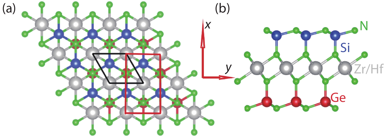
The crystal structure of the Janus monolayer MSiGeN4 (M = Zr and Hf) is shown in Fig. 1 with the rhombus primitive cell and the rectangle supercell marked by black and red frames. With MN2 (M = Zr and Hf) triple layers sandwiched between the SiN and GeN bilayers, the symmetry of Janus monolayer MSiGeN4 (M = Zr and Hf) is lower than that of the MSi2N4 (M = Zr and Hf) or the MGe2N4 (M = Zr and Hf) monolayer due to the lack of the vertical reflection symmetry. In other words, Janus monolayer MSiGeN4 (M = Zr and Hf) can be built by replacing the Si/Ge atoms of the top SiN/GeN bilayer in the MSi2N4/MGe2N4 monolayer with Ge/Si atoms. We use GGA to optimize lattice constants of monolayer MSiGeN4 (M = Zr and Hf), and they are 3.110 and 3.097 Å, which are between the ones of MSi2N4 (3.05 and 3.19 Å) and MGe2N4 (3.04 and 3.18 Å)[
![]()
Figure 1.(Color online) The crystal structures of
The dynamical stability of monolayer MSiGeN4 (M = Zr and Hf) is studied by calculating their phonon band dispersions, which are shown in Fig. 2. It is clearly seen that the phonon branches are free from any imaginary frequencies, indicating the dynamical stability of these monolayers. They exhibit three acoustic and eighteen optical phonon branches due to seven atoms in the unit cell. In addition, the thermal stability is examined by AIMD simulations. During the simulations, the temperature is kept at 600 K, and the temperature and total energy fluctuations of only ZrSiGeN4 monolayer are plotted in Fig. 3 due to similar results between ZrSiGeN4 and HfSiGeN4. The crystal structures of ZrSiGeN4 at 600 K after the simulation for 3 ps are also plotted in Fig. 3. It is found that monolayer ZrSiGeN4 undergoes no structural reconstruction around 600 K, which indicates the thermal stability of these monolayers with the temperature and total energy fluctuating in the acceptable range.
![]()
Figure 2.(Color online)The phonon dispersion curves of
![]()
Figure 3.(Color online) (a) The fluctuations of temperature and total energy with the time obtained from MD simulation of
To verify the mechanical stability of MSiGeN4 (M = Zr and Hf), the investigation of the mechanical properties are carried out. Due to hexagonal symmetry, using Voigt notation, the elastic tensor can be expressed as:
The two independent elastic constants of ZrSiGeN4/HfSiGeN4 are
The 2D Young's moduli
The calculated
The MGe2N4 (M = Zr and Hf) has a lower formation energy than MSi2N4[
Phonon band dispersion calculations, elastic constants and AIMD simulations reveal the dynamical, mechanical and thermal stabilities of predicted monolayers. Monolayer MSi2N4 (M = Mo and W) have been synthesized by introducing Si during CVD growth of M2N (M = Mo and W)[
4. Electronic structure
For Janus MSiGeN4 (M = Mo and W) monolayers, the SOC can produce important effects on their electronic structures, like Rashba spin splitting and valley polarization[
![]()
Figure 4.(Color online) Band structures of
Strain can be used to tune the physical and chemical properties of 2D materials[
![]()
Figure 5.(Color online) Band structures of
![]()
Figure 6.(Color online) The band gaps of
It is found that tensile strain can tune the positions of VBM and CBM of MSiGeN4 (M = Zr and Hf). Tensile strain can make CBM change from M point to Γ point, and VBM move from Γ point to one point along the M–K direction. These lead to that MSiGeN4 (M = Zr and Hf) change from an indirect gap semiconductor to a direct one to an indirect one. For example, a direct gap semiconductor can be observed at 1.04 strain. The Rashba-type spin splitting near the CBM can be induced by tensile strain. At 1.04 strain, the enlarged views of the conduction bands near the Fermi level for MSiGeN4 (M = Zr and Hf) monolayers using GGA+SOC are plotted in Fig. 7. It is clearly seen that a very weak Rashba-type spin splitting is produced. The constant energy 2D contour plots of spin texture of HfSiGeN4 as a representative centered at the Γ point are plotted in Fig. 8 at an energy surface of 1.5 eV above the Fermi level. The spin-up (red) and spin-down (blue) electronic bands can be distinctly observed, which shows the Rashba-type spin splitting. Due to the pure 2D Rashba spin splitting, the concentric spin-texture circles are observed. In the Rashba spin split bands, the only in-plane
![]()
Figure 7.The larger version around CBM for
![]()
Figure 8.(Color online) In-plane spin textures calculated at the iso-energy surface of 1.5 eV above the Fermi level for
5. Piezoelectric properties
The
For MSiGeN4 (M = Mo and W) monolayers, the same reduced piezoelectric stress and strain tensors can be attained[
We use nonprimitive orthorhombic supercells as the computational unit cell (in Fig. 1) to calculate the
6. Optical properties
By calculating the complex dielectric function
where the vacuum dielectric constant, the volume and the energy of the incident phonon are marked by
Here, the rhombus primitive cell is used to calculate the optical properties of MSiGeN4 (M = Mo and W) monolayers. It is well known that the unit-cell volume
![]()
Figure 9.(Color online) The calculated optical dielectric function of
![]()
Figure 10.(Color online) The optical absorption coefficients of
7. Discussions and conclusion
The Janus
In summary, the electronic structures, piezoelectric properties and optical properties of Janus MSiGeN4 (M = Zr and Hf) monolayers are systematically investigated by DFT. They exhibit mechanical, dynamic and thermal stabilities, and show indirect gap properties. It is found that strain can effectively tune their electronic structures, and can induce semiconductors to metal transition in the considered strain range. A very weak Rashba-type spin splitting near CBM can be induced by tensile strain. Both in-plane and out-of-plane piezoelectricity are predicted in MSiGeN4 (M = Zr and Hf) monolayers. The high absorption coefficients in the visible light region can be found along both xx/yy and zz directions. Our works can stimulate further experimental works to synthesize Janus MA2Z4 monolayers, and will motivate farther theoretical studies of other Janus MA2Z4, like
Acknowledgements
This work is supported by Natural Science Basis Research Plan in Shaanxi Province of China (2021JM-456). We are grateful to the Advanced Analysis and Computation Center of China University of Mining and Technology (CUMT) for the award of CPU hours and WIEN2k/VASP software to accomplish this work.
References
[1] L Zhang, Z Yang, T Gong et al. Recent advances in emerging Janus two-dimensional materials: From fundamental physics to device applications. J Mater Chem A, 8, 8813(2020).
[2] A Y Lu, H Y Zhu, J Xiao et al. Janus monolayers of transition metal dichalcogenides. Nat Nanotechnol, 12, 744(2017).
[3] J Zhang, S Jia, I Kholmanov et al. Janus monolayer transition-metal dichalcogenides. ACS Nano, 11, 8192(2017).
[4] S Singh, A H Romero. Giant tunable Rashba spin splitting in a two-dimensional BiSb monolayer and in BiSb/AlN heterostructures. Phys Rev B, 95, 165444(2017).
[5] S D Guo, X S Guo, R Y Han et al. Predicted Janus SnSSe monolayer: A comprehensive first-principles study. Phys Chem Chem Phys, 21, 24620(2019).
[6] Y D Guo, H B Zhang, H L Zeng et al. A progressive metal–semiconductor transition in two-faced Janus monolayer transition-metal chalcogenides. Phys Chem Chem Phys, 20, 21113(2018).
[7] R Peng, Y D Ma, B B Huang et al. Two-dimensional Janus PtSSe for photocatalytic water splitting under the visible or infrared light. J Mater Chem A, 7, 603(2019).
[8] A Mogulkoc, Y Mogulkoc, S Jahangirov et al. Characterization and stability of Janus TiXY (X/Y = S, Se, and Te) monolayers. J Phys Chem C, 123, 29922(2019).
[9] C M Zhang, Y H Nie, S Sanvito et al. First-principles prediction of a room-temperature ferromagnetic Janus VSSe monolayer with piezoelectricity, ferroelasticity, and large valley polarization. Nano Lett, 19, 1366(2019).
[10] Y C Cheng, Z Y Zhu, M Tahir et al. Spin-orbit–induced spin splittings in polar transition metal dichalcogenide monolayers. EPL, 102, 57001(2013).
[11] M L Sun, Q Q Ren, S K Wang et al. Electronic properties of Janus silicene: New direct band gap semiconductors. J Phys D, 49, 445305(2016).
[12] S D Guo, W Q Mu, Y T Zhu et al. Predicted septuple-atomic-layer Janus MSiGeN4 (M = Mo and W) monolayers with Rashba spin splitting and high electron carrier mobilities. J Mater Chem C, 9, 2464(2021).
[13] L Dong, J Lou, V B Shenoy. Large in-plane and vertical piezoelectricity in Janus transition metal dichalchogenides. ACS Nano, 11, 8242(2017).
[14] M Yagmurcukardes, C Sevik, F M Peeters. Electronic, vibrational, elastic, and piezoelectric properties of monolayer Janus MoSTe phases: A first-principles study. Phys Rev B, 100, 045415(2019).
[15] W H Zhou, S L Zhang, S Y Guo et al. Designing sub-10-nm metal-oxide-semiconductor field-effect transistors via ballistic transport and disparate effective mass: The case of two-dimensional BiN. Phys Rev Appl, 13, 044066(2020).
[16] W H Zhou, S L Zhang, Y Y Wang et al. Anisotropic in-plane ballistic transport in monolayer black arsenic- phosphorus FETs. Adv Electron Mater, 6, 1901281(2020).
[17] Y L Hong, Z Liu, L Wang et al. Chemical vapor deposition of layered two-dimensional MoSi2N4 materials. Science, 369, 670(2020).
[18] L Wang, Y P Shi, M F Liu et al. Intercalated architecture of MA2Z4 family layered van der Waals materials with emerging topological, magnetic and superconducting properties. Nat Commun, 12, 2361(2021).
[19] S Li, W K Wu, X L Feng et al. Valley-dependent properties of monolayer MoSi2N4, WSi2N4, and MoSi2As4. Phys Rev B, 102, 235435(2020).
[20] C Yang, Z G Song, X T Sun et al. Valley pseudospin in monolayer MoSi2N4 and MoSi2As4. Phys Rev B, 103, 035308(2021).
[21] S D Guo, Y T Zhu, W Q Mu et al. Intrinsic piezoelectricity in monolayer MSi2N4 (M = Mo, W, Cr, Ti, Zr and Hf). EPL, 132, 57002(2020).
[22] S D Guo, Y T Zhu, W Q Mu et al. Structure effect on intrinsic piezoelectricity in septuple-atomic-layer MSi2N4 (M = Mo and W). Comput Mater Sci, 188, 110223(2021).
[23] S D Guo, W Q Mu, Y T Zhu et al. Coexistence of intrinsic piezoelectricity and ferromagnetism induced by small biaxial strain in septuple-atomic-layer VSi2P4. Phys Chem Chem Phys, 22, 28359(2020).
[24] L M Cao, G H Zhou, Q Q Wang et al. Two-dimensional van der Waals electrical contact to monolayer MoSi2N4. Appl Phys Lett, 118, 013106(2021).
[25] J H Yu, J Zhou, X G Wan et al. High intrinsic lattice thermal conductivity in monolayer MoSi2N4. New J Phys, 23, 033005(2021).
[26] P Hohenberg, W Kohn. Inhomogeneous electron gas. Phys Rev, 136, B864(1964).
[27] G Kresse. Ab initio molecular dynamics for liquid metals. J Non Cryst Solids, 192/193, 222(1995).
[28] G Kresse, J Furthmüller. Efficiency of ab-initio total energy calculations for metals and semiconductors using a plane-wave basis set. Comput Mater Sci, 6, 15(1996).
[29] G Kresse, D Joubert. From ultrasoft pseudopotentials to the projector augmented-wave method. Phys Rev B, 59, 1758(1999).
[30] J P Perdew, K Burke, M Ernzerhof. Generalized gradient approximation made simple. Phys Rev Lett, 77, 3865(1996).
[31] A Togo, F Oba, I Tanaka. First-principles calculations of the ferroelastic transition between rutile-type and CaCl2-type SiO2 at high pressures. Phys Rev B, 78, 134106(2008).
[32] U Herath, P Tavadze, X He et al. PyProcar: A Python library for electronic structure pre/post-processing. Comput Phys Commun, 251, 107080(2020).
[33] X F Wu, D Vanderbilt, D R Hamann. Systematic treatment of displacements, strains, and electric fields in density-functional perturbation theory. Phys Rev B, 72, 035105(2005).
[34] G Y Guo, K C Chu, D S Wang et al. Linear and nonlinear optical properties of carbon nanotubes from first-principles calculations. Phys Rev B, 69, 205416(2004).
[35] R C Andrew, R E Mapasha, A M Ukpong et al. Erratum: Mechanical properties of graphene and boronitrene [Phys. Rev. B 85, 125428 (2012)]. Phys Rev B, 69, 205416(2004).
[36] M N Blonsky, H L Zhuang, A K Singh et al. Ab initio prediction of piezoelectricity in two-dimensional materials. ACS Nano, 9, 9885(2015).
[37] R X Fei, W B Li, J Li et al. Giant piezoelectricity of monolayer group IV monochalcogenides: SnSe, SnS, GeSe, and GeS. Appl Phys Lett, 107, 173104(2015).
[38] K A N Duerloo, M T Ong, E J Reed. Intrinsic piezoelectricity in two-dimensional materials. J Phys Chem Lett, 3, 2871(2012).
[39] Z Q Fan, X W Jiang, Z M Wei et al. Tunable electronic structures of GeSe nanosheets and nanoribbons. J Phys Chem C, 121, 14373(2017).
[40] X X Xue, Y X Feng, L Liao et al. Strain tuning of electronic properties of various dimension elemental tellurium with broken screw symmetry. J Phys: Condens Matter, 30, 125001(2018).
[41] S D Guo, J Dong. Biaxial strain tuned electronic structures and power factor in Janus transition metal dichalchogenide monolayers. Semicond Sci Technol, 33, 085003(2018).
[42] M Gajdoš, K Hummer, G Kresse et al. Linear optical properties in the projector-augmented wave methodology. Phys Rev B, 73, 045112(2006).
[43] X Huang, T R Paudel, S Dong et al. Hexagonal rare-earth manganites as promising photovoltaics and light polarizers. Phys Rev B, 92, 125201(2015).


Set citation alerts for the article
Please enter your email address

© Copyright 2018-2021 | Chinese Laser Press. All Rights Reserved 沪ICP备15018463号-20