• Photonics Research
  • Vol. 4, Issue 1, 0021 (2016)
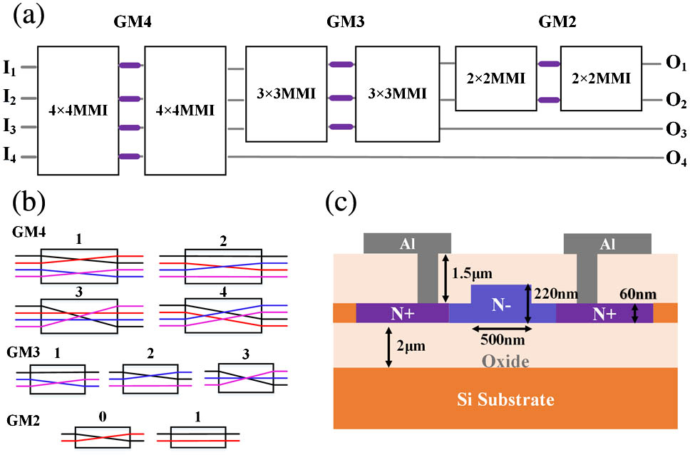
Zuxiang Li, Linjie Zhou*, Liangjun Lu, Shuoyi Zhao, Dong Li, and Jianping Chen
Author Affiliations
  • State Key Laboratory of Advanced Optical Communication Systems and Networks, Department of ElectronicEngineering, Shanghai Jiao Tong University, Shanghai 200240, China
  • show less
    DOI: 10.1364/prj.4.000021 Cite this Article Set citation alerts
    Zuxiang Li, Linjie Zhou, Liangjun Lu, Shuoyi Zhao, Dong Li, Jianping Chen. 4 × 4 nonblocking optical switch fabric based on cascaded multimode interferometers[J]. Photonics Research, 2016, 4(1): 0021 Copy Citation Text show less
    (a) Structure of the 4×4 switch based on cascaded GMZIs. (b) All switching states of single 4×4, 3×3, and 2×2 GMZIs. (c) Cross-sectional schematic of the TO phase shifter.
    Fig. 1. (a) Structure of the 4×4 switch based on cascaded GMZIs. (b) All switching states of single 4×4, 3×3, and 2×2 GMZIs. (c) Cross-sectional schematic of the TO phase shifter.
    (a) Optical microscope image of the fabricated 4×4 switch. (b) Zoom-in view of the GMZI switch element. (c) Home-packaged switch chip.
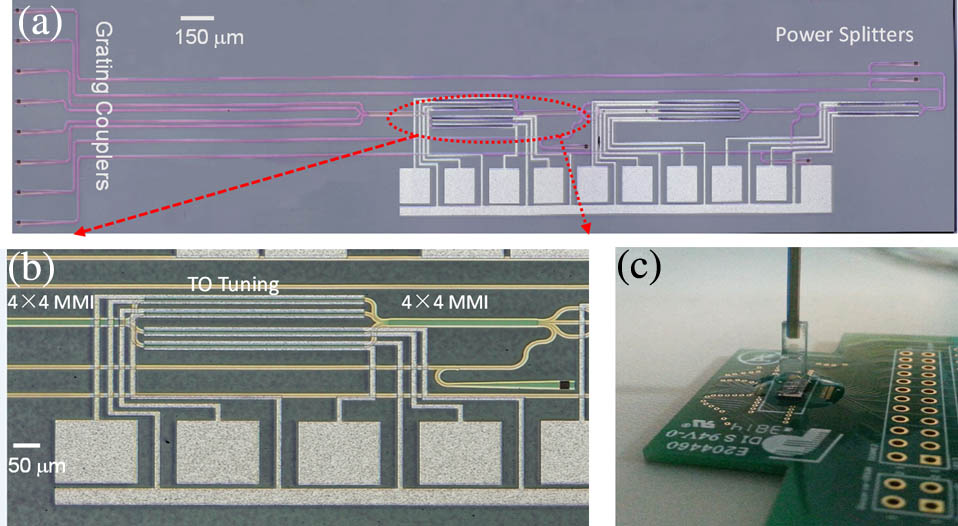
    Fig. 2. (a) Optical microscope image of the fabricated 4×4 switch. (b) Zoom-in view of the GMZI switch element. (c) Home-packaged switch chip.
    Measured transmission spectra for state ID=3.
    Fig. 3. Measured transmission spectra for state ID=3.
    Measured transmission spectra for state ID=22.
    Fig. 4. Measured transmission spectra for state ID=22.
    Histogram of on-chip insertion loss of all 24 states.
    Fig. 5. Histogram of on-chip insertion loss of all 24 states.
    Histogram of cross talk of all 24 states.
    Fig. 6. Histogram of cross talk of all 24 states.
    Experimental setup for optical data transmission measurement.
    Fig. 7. Experimental setup for optical data transmission measurement.
    Measured eye diagrams of a 25 Gb/s OOK signal before and after the switch chip. (a) BtB transmission, (b) switching state ID=3, and (c) switching state ID=22.
    Fig. 8. Measured eye diagrams of a 25 Gb/s OOK signal before and after the switch chip. (a) BtB transmission, (b) switching state ID=3, and (c) switching state ID=22.
    Tolerance analysis of power imbalance of the 4×4 and 3×3 MMIs on the cross talk of the device. The triangle represents the simulation of our fabricated device.
    Fig. 9. Tolerance analysis of power imbalance of the 4×4 and 3×3 MMIs on the cross talk of the device. The triangle represents the simulation of our fabricated device.
    State IDGM4GM3GM2O1O2O3O4TO Power
    1310I3I4I2I1102.31
    2311I4I3I2I1124.69
    3320I4I2I3I1107.64
    4321I2I4I3I1126.96
    5330I2I3I4I1107.64
    6331I3I2I4I1124.26
    7410I1I3I4I278.73
    8411I3I1I4I2101.11
    9420I3I4I1I284.06
    10421I4I3I1I2103.38
    11430I4I1I3I281.36
    12431I1I4I3I296.34
    13110I4I2I1I372.16
    14111I2I4I1I394.67
    15120I2I1I4I362.23
    16121I1I2I4I377.21
    17130I1I4I2I362.29
    18131I4I1I2I377.27
    19210I2I1I3I4123.53
    20211I1I2I3I4145.91
    21220I1I3I2I4122.75
    22221I3I1I2I4142.07
    23230I3I2I1I4126.16
    24231I2I3I1I4141.14
    Table 1. All Switching States and Corresponding Power Consumptiona
    Zuxiang Li, Linjie Zhou, Liangjun Lu, Shuoyi Zhao, Dong Li, Jianping Chen. 4 × 4 nonblocking optical switch fabric based on cascaded multimode interferometers[J]. Photonics Research, 2016, 4(1): 0021
    Download Citation