Abstract
We experimentally demonstrate a 4 × 4 nonblocking silicon thermo-optic (TO) switch fabric consisting of three stages of tunable generalized Mach–Zehnder interferometers. All 24 routing states for nonblocking switching are characterized. The device’s footprint is 4.6 mm × 1.0 mm. Measurements show that the worst cross talk of all switching states is ?7.2 dB. The on-chip insertion loss is in the range of 3.7–13.1 dB. The average TO switching power consumption is 104.8 mW.1. INTRODUCTION
Continuous increase in the network traffic for optical communications and inter- and intro-chip interconnects demand vast development of all-optical switches [1–3]. The requirement for optical switches includes large port count, low power consumption, nonblocking, and low cost. Recently, strictly nonblocking thermo-optic (TO) optical switches based on Si waveguides [4] and monolithically integrated digital silicon photonic switches with MEMS actuation [5] have been demonstrated. The former employs a path-independent-insertion-loss topology and is composed of 1024 switch elements and 961 waveguide intersections. The later consists of 2500 () switching cells based on a crossbar architecture with a MEMS actuator for each element. The operational voltage is relatively high, ranging from 22 to 32 V.
An optical switch is usually constructed by or switch elements, such as Mach–Zehnder interferometers (MZIs), microring resonators, and directional couplers [1–10]. MZI-based switches have a broad optical bandwidth and good tolerance to environmental temperature variations [11,12]. Multimode interference (MMI) couplers, based on the self-imaging effect, function as efficient splitters and combiners for optical beams. They are widely used in MZIs [13–15] because they possess the desirable attributes of small size, low excess loss, well-defined splitting ratio, dimensional tolerance, and ease of fabrication [16,17]. Benefiting from these merits, MMI couplers have been used as building blocks for more complex structures. For instance, a generalized Mach–Zehnder interferometer (GMZI) can be formed by connecting multiport MMIs using an array of phase shifters [16,18]. and GMZI switches have been recently demonstrated [19,20]. Unfortunately, a single GMZI can only provide independent switching states [18]; thus, it is a blocking switch. A nonblocking switch could be realized by cascading several stages of GMZIs. In our previous work [11], we have demonstrated a silicon nonblocking switch by cascading four GMZIs on both sides of a GMZI to form a balanced structure. It has five GMZI switch elements in total.
In this paper, we report the realization of an alternative GMZI-based switch where , , and MMI pairs are cascaded in series. Compared with our previous work, it has three GMZI switch elements, resulting in a more compact structure and less phase shifters. As far as we know, there have been no experimental demonstrations of such kind of GMZI switches in the literature. The GMZI switch is nonblocking and of no waveguide intersections. The footprint of the switch chip is . The worst cross talk for all switching states is . The switching function is verified by transmission of a 25 Gb/s on–off keying (OOK) optical signal. Section 2 offers details of the switch architecture and fabrication. Section 3 presents the experimental characterization of the device. Section 4 draws the conclusions.
Sign up for Photonics Research TOC. Get the latest issue of Photonics Research delivered right to you!Sign up now
2. DEVICE DESIGN AND FABRICATION
Figure 1(a) shows the switch architecture consisting of three stages of GMZIs. The cascaded architecture requires the minimum number of switch elements to obtain the full 24 switching states for nonblocking operation. For the GMZI structure, when one connection is established, the other three connections for a particular switching state is uniquely defined. As a consequence, the GMZI (GM4) in Fig. 1(a) has only four switching states. To achieve the full connections, we cascade a GMZI (GM3) and a GMZI (GM2) in series at the end of the GM4. This cascaded structure can generate permutations to form a nonblocking switch. The sizes () of the , , and MMIs are , , and , respectively. It should be noted that the routing paths are not balanced. Light to only goes through GM4, resulting in a lower loss. Figure 1(b) shows all the possible switching states for the , , and GMZIs.
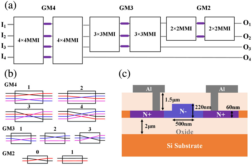
Figure 1.(a) Structure of the switch based on cascaded GMZIs. (b) All switching states of single , , and GMZIs. (c) Cross-sectional schematic of the TO phase shifter.
Two routinely used approaches are used to tune the refractive index of silicon based on either the TO effect or the free-carrier plasma dispersion effect [21]. The former approach is relatively strong, as silicon has a large TO coefficient of at 300 K. No excess loss is incurred upon TO tuning, but the switching speed is in the order of μs. The latter approach, comparatively, is fast, but the change of refractive index is small, limited by the free-carrier absorption loss. In our switch, we integrate TO phase shifters made of silicon-resistive microheaters into the arms of all GMZIs [22]. When current flows through the waveguide, heat will be generated and interact directly with the waveguide mode without the heat diffusion process, as in a conventional metal-based microheater, hence providing a more effective way to tune the phase. Figure 1(c) shows the cross-sectional schematic of the silicon resistive microheater. The silicon waveguide has a dimension of with a slab thickness of 0.06 μm. The highly -doped regions have a doping concentration of and are separated from the waveguide by 0.8 μm to ensure low free-carrier absorption. The waveguide is slightly -doped with a concentration of to reduce the resistance of the microheater while maintaining a low propagation loss.
The GMZI-based switch can be modeled using the transfer matrix method. The total transfer matrix of the switch is a multiplication of the constituted GMZI matrices:
The GMZI matrix consists of the splitter matrix , the phase shifter matrix , and the combiner matrix where , 3, 4:
The phase shifters are driven independently, and they can be described by a diagonal transfer matrix:
The ideal transfer matrices for the , , and MMIs are given by [16]
It should be noted that the transfer matrices for the and MMIs are expanded to matrices with the connections shown in Fig. 1(a).
The switch was fabricated on a silicon-on-insulator wafer. Silicon waveguides were patterned using 248 nm photolithography and etched using reactive ion etch. Rapid thermal annealing at 1030°C for 5 s was performed after ion implantation to form the and doped regions. Then, a 1.5 μm thick oxide was deposited on waveguides using the plasma-enhanced chemical vapor deposition as upper cladding. Finally, contact holes were etched, and an aluminum connection was formed by sputtering and plasma dry etch. The whole fabrication process was CMOS compatible.
Figure 2(a) shows the optical microscope image of the fabricated switch. The size of the device is , including all the electrical pads and fiber array coupling region. Grating couplers with a 0.63 μm period and a 0.07 μm shallow etch depth are used for input and output coupling. In our design, a directional coupler is inserted into each output waveguide so that light can be coupled out of the chip from the left side (fiber array coupling) and the right side (individual fiber coupling) to facilitate chip testing and package. The splitting loss at the fiber array end is about 4.8 dB. Figure 2(b) shows the magnified image of the switch element GM4. The MMIs are connected using unbalanced waveguide arms. The metal pads are wire-bonded to a printed circuit board. An eight-channel fiber array is aligned and attached to the chip by using ultraviolet light curable adhesive, whose refractive index is close to the refractive index of . Figure 2(c) shows the photo of the home-packaged switch chip.

Figure 2.(a) Optical microscope image of the fabricated switch. (b) Zoom-in view of the GMZI switch element. (c) Home-packaged switch chip.
3. EXPERIMENTAL RESULTS
A routing path from an input port to a specific output port is established by applying proper voltages onto the TO phase shifters. Due to the incomplete interference, light from one input port also could partially leak to the other three output ports beside the destination, leading to interchannel cross talk. For each switching state, we record the transmitted power for all main and leakage paths to derive the insertion loss and cross talk. The TO power consumption of each switching state is measured and listed in Table 1. As the GMZI is essentially an interference structure, only the relative phases are crucial to set the switching state. Therefore, we leave one arm in each GMZI [the top arm in Fig. 1(a)] without tuning to save power consumption. As shown in the table, the minimum power is 62.23 mW, the maximum is 145.91 mW, and the average is 104.84 mW. The power consumption can be further reduced by using isolation grooves to minimize thermal leakage [19].
| State ID | GM4 | GM3 | GM2 | O1 | O2 | O3 | O4 | TO Power |
|---|
| 1 | 3 | 1 | 0 | I3 | I4 | I2 | I1 | 102.31 |
| 2 | 3 | 1 | 1 | I4 | I3 | I2 | I1 | 124.69 |
| 3 | 3 | 2 | 0 | I4 | I2 | I3 | I1 | 107.64 |
| 4 | 3 | 2 | 1 | I2 | I4 | I3 | I1 | 126.96 |
| 5 | 3 | 3 | 0 | I2 | I3 | I4 | I1 | 107.64 |
| 6 | 3 | 3 | 1 | I3 | I2 | I4 | I1 | 124.26 |
| 7 | 4 | 1 | 0 | I1 | I3 | I4 | I2 | 78.73 |
| 8 | 4 | 1 | 1 | I3 | I1 | I4 | I2 | 101.11 |
| 9 | 4 | 2 | 0 | I3 | I4 | I1 | I2 | 84.06 |
| 10 | 4 | 2 | 1 | I4 | I3 | I1 | I2 | 103.38 |
| 11 | 4 | 3 | 0 | I4 | I1 | I3 | I2 | 81.36 |
| 12 | 4 | 3 | 1 | I1 | I4 | I3 | I2 | 96.34 |
| 13 | 1 | 1 | 0 | I4 | I2 | I1 | I3 | 72.16 |
| 14 | 1 | 1 | 1 | I2 | I4 | I1 | I3 | 94.67 |
| 15 | 1 | 2 | 0 | I2 | I1 | I4 | I3 | 62.23 |
| 16 | 1 | 2 | 1 | I1 | I2 | I4 | I3 | 77.21 |
| 17 | 1 | 3 | 0 | I1 | I4 | I2 | I3 | 62.29 |
| 18 | 1 | 3 | 1 | I4 | I1 | I2 | I3 | 77.27 |
| 19 | 2 | 1 | 0 | I2 | I1 | I3 | I4 | 123.53 |
| 20 | 2 | 1 | 1 | I1 | I2 | I3 | I4 | 145.91 |
| 21 | 2 | 2 | 0 | I1 | I3 | I2 | I4 | 122.75 |
| 22 | 2 | 2 | 1 | I3 | I1 | I2 | I4 | 142.07 |
| 23 | 2 | 3 | 0 | I3 | I2 | I1 | I4 | 126.16 |
| 24 | 2 | 3 | 1 | I2 | I3 | I1 | I4 | 141.14 |
Table 1. All Switching States and Corresponding Power Consumptiona
Figures 3 and 4 show the measured normalized transmission spectra for two typical switching states. In each plot, the transverse electric (TE) polarized light is launched from four input ports, and the spectra from one output port were recorded. Because of the imbalanced arms between MMIs, the spectra exhibit periodic interference patterns. The switch operation wavelength is set around 1533 nm.
Figure 3.Measured transmission spectra for state .
Figure 4.Measured transmission spectra for state .
From the spectra of the two switching states, one observes that the transmission to has the lowest loss, which is expected, as light only goes through GM4. As we used the 3D beam propagation method to design the device, it may not be accurate enough for the high index contrast silicon waveguides. The insertion loss of the switch fabric would be reduced if the MMIs were optimized using the 3D finite-difference time-domain method.
Figure 5 shows the histogram of on-chip insertion loss of all the 24 states. The on-chip insertion loss is varied from 3.7 to 13.1 dB. The variation of on-chip insertion loss comes from the unbalanced routing paths and uneven splitting ratio of MMIs. Variable optical attenuators could be integrated into output waveguides to adjust the output optical power [23].
Figure 5.Histogram of on-chip insertion loss of all 24 states.
The cross talk induced by the input port to the routing path (, , 2, 3, and 4) is defined as the ratio of leaked output power to the output power [11]. According to this definition, for one specific routing path, the leaked power may come from the other three input ports. There are a total of cross-talk values for all switching states. The device cross talk is then defined as the worst cross talk of all routing paths. Figure 6 shows the histogram of cross talk of all the switching states. As shown in Fig. 6, the cross talk varies between , with an average around . Compared with our previous work [11], the MMIs in this switch fabric have larger output power imbalance, leading to the wider spread of insertion loss and cross talk over different routing paths.
Figure 6.Histogram of cross talk of all 24 states.
We performed an optical data transmission experiment using a 25 Gb/s OOK signal to verify the signal fidelity after switching. Figure 7 shows the experimental setup for data transmission. A tunable laser source generates a continuous wave light at 1533 nm wavelength and is then modulated by an intensity modulator to generate the OOK signal. The modulator is driven by a pulse-pattern generator with a 25 Gb/s eudo-random bit sequence radio frequency signal. The modulated optical signal is then amplified by an erbium-doped fiber amplifier (EDFA) and goes through a polarization controller to set the TE polarization before it is coupled into the chip. The output optical signal is then amplified by another EDFA followed by a bandpass filter to compensate for the loss of the chip. The switched signal is finally received by a photodetector (PD) and analyzed by the DCA-X wide-bandwidth oscilloscope (Keysight, DCA-X 86100D).
Figure 7.Experimental setup for optical data transmission measurement.
Figure 8(a) shows the back-to-back (BtB) eye diagram of the test system, where the input optical signal is directly received the PD. Figures 8(b) and 8(c) depict the eye diagrams from the four output ports after transmission through the switch chip. All eye diagrams are clearly open. The output signal experiences almost no deterioration in the extinction ratio. It demonstrates that our nonblocking switch has the capacity to switch a 25 Gb/s OOK signal with good signal fidelity.
Figure 8.Measured eye diagrams of a 25 Gb/s OOK signal before and after the switch chip. (a) BtB transmission, (b) switching state , and (c) switching state .
4. DISCUSSION
We use the transfer matrix with random error statistics to estimate the cross talk of this switch. The power imbalance of the MMIs is the main source for the deterioration of switch cross talk [11]. Here, the power imbalance of a MMI refers to the uneven splitting ratio when light is incident from one input port [19]. We consider the effect of power and phase random variation in each MMI output port on the device performances. The elements , , and in the transfer matrices of , , and MMIs can be written as [11,19] where , , and are the ideal phases of , , and MMIs, respectively. The three variables , , and set the maximum output power variation of the , , and MMIs, respectively. The expression rand() stands for a random number between 0 and 1.
With the phase shifters in the GMZIs are set for a certain state, the cross talk of each routing path can be derived from the switch matrix given by Eq. (1). As defined, the worst of all routing paths is the switch cross talk. We repeat the process 1000 times with random power and phase variations to obtain the average cross talk. The result is shown in Fig. 9. We set the power imbalance of the MMI as 0.01 dB [11]. The power imbalance the and the MMIs is much larger than the MMI and is the main contribution to the cross talk. Using the eigenmode expansion method, we obtain the power imbalance of the and MMIs as 1.26 and 1.56 dB, respectively. This leads to about cross talk according to our model, as shown in Fig. 9, which is consistent with the experimental result. One sees that, in order to obtain a cross talk below , the power imbalance must be kept below 0.6 and 0.5 dB for the and MMIs, respectively.
Figure 9.Tolerance analysis of power imbalance of the and MMIs on the cross talk of the device. The triangle represents the simulation of our fabricated device.
5. CONCLUSION
We have demonstrated a nonblocking silicon TO switch based on cascaded GMZIs. Experimental results show that the on-chip insertion loss is in the range of 3.7 to 13.1 dB. The average cross talk is around with the worst value of . The average TO power consumption is 104.84 mW. The performance of the optical switch can be further improved by optimizing the and and MMIs with lower insertion loss and a more uniform power splitting ratio.
Acknowledgment
Acknowledgment. This work was supported in part by the 863 program (2013AA014402), the National Natural Science Foundation of China (NSFC) (61422508), and the Science and Technology Commission of Shanghai Municipality (STCSM) Project (14QA1402600). We also acknowledge IME Singapore for device fabrication.
References
[1] B. G. Lee, A. V. Rylyakov, W. M. J. Green, S. Assefa, C. W. Baks, R. Rimolo-Donadio, D. M. Kuchta, M. H. Khater, T. Barwicz, C. Reinholm, E. Kiewra, S. M. Shank, C. L. Schow, Y. A. Vlasov. Monolithic silicon integration of scaled photonic switch fabrics, CMOS logic, and device driver circuits. J. Lightwave Technol., 32, 743-751(2014).
[2] K. Suzuki, K. Tanizawa, T. Matsukawa, G. Cong, S. H. Kim, S. Suda, M. Ohno, T. Chiba, H. Tadokoro, M. Yanagihara, Y. Igarashi, M. Masahara, S. Namiki, H. Kawashima. Ultra-compact 8×8 strictly-non-blocking Si-wire PILOSS switch. Opt. Express, 22, 3887-3894(2014).
[3] L. Zhou, L. Lu, Z. Li, J. Chen. Broadband 4×4 non-blocking optical switch fabric based on Mach–Zehnder interferometers. 13th International Conference on Optical Communications and Networks, 1-4(2014).
[4] K. Tanizawa, K. Suzuki, M. Toyama, M. Ohtsuka, N. Yokoyama, K. Matsumaro, M. Seki, K. Koshino, T. Sugaya, S. Suda, G. Cong, T. Kimura, K. Ikeda, S. Namiki, H. Kawashima. 32×32 strictly non-blocking si-wire optical switch on ultra-small die of 11×25 mm2. Optical Fiber Communication Conference, M2B.5(2015).
[5] T. J. Seok, N. Quack, S. Han, M. C. Wu. 50×50 digital silicon photonic switches with MEMS-actuated adiabatic couplers. Optical Fiber Communication Conference, M2B.4(2015).
[6] J. Xing, Z. Li, P. Zhou, X. Xiao, J. Yu, Y. Yu. Nonblocking 4×4 silicon electro-optic switch matrix with push-pull drive. Opt. Lett., 38, 3926-3929(2013).
[7] M. Yang, W. M. Green, S. Assefa, J. Van Campenhout, B. G. Lee, C. V. Jahnes, F. E. Doany, C. L. Schow, J. A. Kash, Y. A. Vlasov. Non-blocking 4×4 electro-optic silicon switch for on-chip photonic networks. Opt. Express, 19, 47-54(2011).
[8] N. Sherwood-Droz, H. Wang, L. Chen, B. G. Lee, A. Biberman, K. Bergman, M. Lipson. Optical 4×4 hitless silicon router for optical networks-on-chip (NoC). Opt. Express, 16, 15915(2008).
[9] A. W. Poon, X. Luo, F. Xu, H. Chen. Cascaded microresonator-based matrix switch for silicon on-chip optical interconnection. Proc. IEEE, 97, 1216-1238(2009).
[10] L. Yang, Y. Xia, F. Zhang, Q. Chen, J. Ding, P. Zhou, L. Zhang. Reconfigurable nonblocking 4-port silicon thermo-optic optical router based on Mach–Zehnder optical switches. Opt. Lett., 40, 1402-1405(2015).
[11] L. Lu, L. Zhou, S. Li, Z. Li, X. Li, J. Chen. 4×4 nonblocking silicon thermo-optic switches based on multimode interferometers. J. Lightwave Technol., 33, 857-864(2015).
[12] Y. Li, Y. Zhang, L. Zhang, A. W. Poon. Silicon and hybrid silicon photonic devices for intra-datacenter applications: state of the art and perspectives Invited.. Photon. Res., 3, B10(2015).
[13] J. Xing, Z. Li, Y. Yu, J. Yu. Low cross-talk 2×2 silicon electro-optic switch matrix with a double-gate configuration. Opt. Lett., 38, 4774-4776(2013).
[14] N. Xie, T. Hashimoto, K. Utaka. Design and performance of low-power, high-speed, polarization-independent and wideband polymer buried- channel waveguide thermo-optic switches. J. Lightwave Technol., 32, 3067-3073(2014).
[15] L. Lu, L. Zhou, X. Li, J. Chen. Low-power 2×2 silicon electro-optic switches based on double-ring assisted Mach–Zehnder interferometers. Opt. Lett., 39, 1633-1636(2014).
[16] N. S. Lagali, M. R. Paiam, R. I. MacDonald, K. Worhoff, A. Driessen. Analysis of generalized Mach-Zehnder interferometers for variable-ratio power splitting and optimized switching. J. Lightwave Technol., 17, 2542-2550(1999).
[17] P. E. Morrissey, H. Yang, R. N. Sheehan, B. Corbett, F. H. Peters. Design and fabrication tolerance analysis of multimode interference couplers. Opt. Commun., 340, 26-32(2015).
[18] L. W. Cahill. The modelling of integrated optical power splitters and switches based on generalised Mach–Zehnder devices. Opt. Quantum Electron., 36, 165-173(2004).
[19] H. Zhou, J. Song, E. K. Chee, C. Li, H. Zhang, G. Lo. A compact thermo-optical multimode-interference silicon-based 1×4 nano-photonic switch. Opt. Express, 21, 21403-21413(2013).
[20] W. Wang, H. Zhou, J. Yang, M. Wang, X. Jiang. Highly integrated 3×3 silicon thermo-optical switch using a single combined phase shifter for optical interconnects. Opt. Lett., 37, 2307-2309(2012).
[21] G. T. Reed, A. P. Knights. Silicon Photonics(2008).
[22] L. Zhou, X. Zhang, L. Lu, J. Chen. Tunable vernier microring optical filters with p-i-p type microheaters. IEEE Photon. J., 5, 6601211(2013).
[23] Q. Wu, L. Zhou, X. Sun, H. Zhu, L. Lu, J. Chen. Silicon thermo-optic variable optical attenuators based on Mach–Zehnder interference structures. Opt. Commun., 341, 69-73(2015).

