• Photonics Research
  • Vol. 6, Issue 7, 692 (2018)
Sheng-Xuan Xia, Xiang Zhai, Ling-Ling Wang*, and Shuang-Chun Wen
Author Affiliations
  • Key Laboratory for Micro-Nano Optoelectronic Devices of Ministry of Education, School of Physics and Electronics, Hunan University, Changsha 410082, China
  • show less
    DOI: 10.1364/PRJ.6.000692 Cite this Article Set citation alerts
    Sheng-Xuan Xia, Xiang Zhai, Ling-Ling Wang, Shuang-Chun Wen. Plasmonically induced transparency in double-layered graphene nanoribbons[J]. Photonics Research, 2018, 6(7): 692 Copy Citation Text show less
    Schematic of the PIT system. Two layers of periodic GNRs with crossed ribbon directions are placed parallel to the x−y plane; the upper and lower layers have ribbon widths W1 and W2 and transverse periods Λ1 and Λ2, respectively. The layers are separated by a distance d. The ribbon layers are assumed to be separated by a conductive Si or SiO2 spacer with refractive index n2 and further covered by two independent ion-gel gates with refractive indices n1=n3. The Fermi levels of the GNRs can be tuned simultaneously by applying two independent bias voltages between the two top gold gates and the conductive spacer. A normally incident plane wave with wave number β0 and polarization angle θ with respect to the x axis strikes the surface of the periodically structured graphene system.
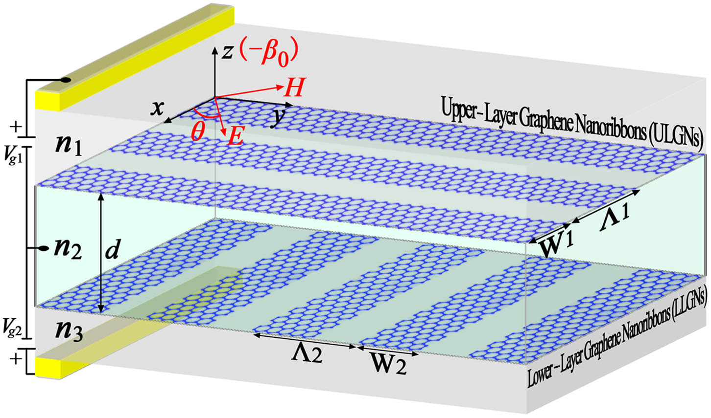
    Fig. 1. Schematic of the PIT system. Two layers of periodic GNRs with crossed ribbon directions are placed parallel to the xy plane; the upper and lower layers have ribbon widths W1 and W2 and transverse periods Λ1 and Λ2, respectively. The layers are separated by a distance d. The ribbon layers are assumed to be separated by a conductive Si or SiO2 spacer with refractive index n2 and further covered by two independent ion-gel gates with refractive indices n1=n3. The Fermi levels of the GNRs can be tuned simultaneously by applying two independent bias voltages between the two top gold gates and the conductive spacer. A normally incident plane wave with wave number β0 and polarization angle θ with respect to the x axis strikes the surface of the periodically structured graphene system.
    (a) Transmission and (b) absorption spectra of the structure with normal incidence and polarization angle θ=0°. Solid green curves and symbols represent the analytical and numerical results, respectively. (c) Transmission phase (left vertical axis) and delay time (right vertical axis) of the spectra shown in (a) and (b).
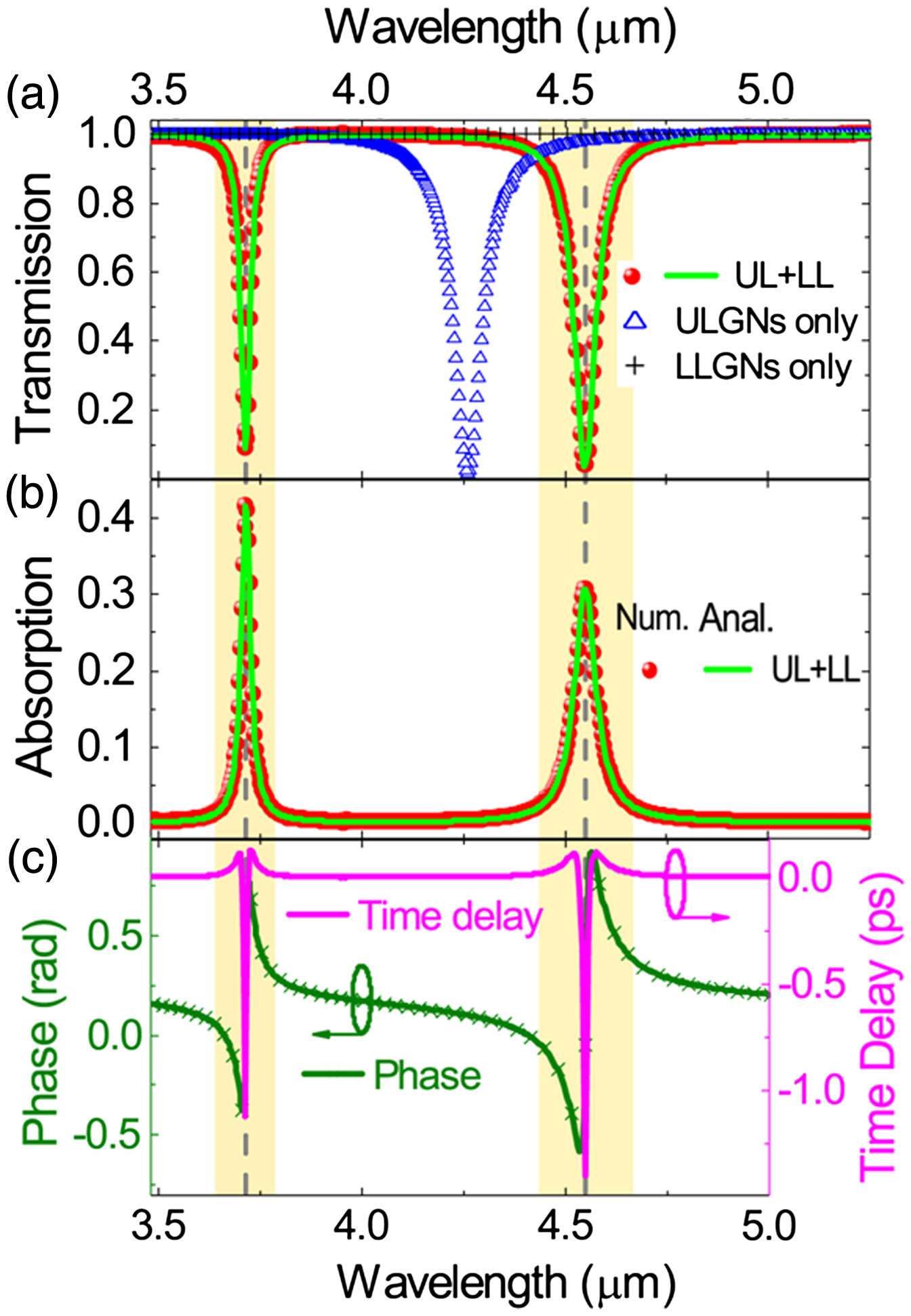
    Fig. 2. (a) Transmission and (b) absorption spectra of the structure with normal incidence and polarization angle θ=0°. Solid green curves and symbols represent the analytical and numerical results, respectively. (c) Transmission phase (left vertical axis) and delay time (right vertical axis) of the spectra shown in (a) and (b).
    Two-dimensional plots of normal-incidence transmission showing the wavelength versus the polarization angle θ for the proposed system with (a) only ULGNRs (upper panel) and only LLGNRs (lower panel) and (b) two-layer GNRs. The left inset in (a) shows the Ez component of the incoming beam at 4.26 µm with only ULGNRs; the right inset plots the transmission dips for only ULGNRs (dark line) and only LLGNRs (red line) versus the polarization angle θ. The inset in (b) depicts the transmission dips of the QAM and QSM versus the polarization angle θ. Spatial distributions of (c)–(e), (i)–(k) the electric field and (f)–(h), (l)–(n) the corresponding z component of the (c)–(h) QAMs and (i)–(n) QSMs at polarization angles θ of (c), (f), (i), (l) 0°, (d), (g), (j), (m) 45°, and (e), (h), (k), (n) 90°. Plus and minus signs denote the oscillating surface charges; darker color represents higher charge density.
    Fig. 3. Two-dimensional plots of normal-incidence transmission showing the wavelength versus the polarization angle θ for the proposed system with (a) only ULGNRs (upper panel) and only LLGNRs (lower panel) and (b) two-layer GNRs. The left inset in (a) shows the Ez component of the incoming beam at 4.26 µm with only ULGNRs; the right inset plots the transmission dips for only ULGNRs (dark line) and only LLGNRs (red line) versus the polarization angle θ. The inset in (b) depicts the transmission dips of the QAM and QSM versus the polarization angle θ. Spatial distributions of (c)–(e), (i)–(k) the electric field and (f)–(h), (l)–(n) the corresponding z component of the (c)–(h) QAMs and (i)–(n) QSMs at polarization angles θ of (c), (f), (i), (l) 0°, (d), (g), (j), (m) 45°, and (e), (h), (k), (n) 90°. Plus and minus signs denote the oscillating surface charges; darker color represents higher charge density.
    Transmission maps of the system at a polarization angle θ of 0° showing the incident wavelength versus (a) the ribbon width W1 of the ULGNRs, (b) the ribbon width W2 of the LLGNRs, and (c) the distance d between the two layers.
    Fig. 4. Transmission maps of the system at a polarization angle θ of 0° showing the incident wavelength versus (a) the ribbon width W1 of the ULGNRs, (b) the ribbon width W2 of the LLGNRs, and (c) the distance d between the two layers.
    (a) Two-dimensional transmission map of the system plotted as the wavelength versus the Fermi level EF. The inset, which has the same coordinates as the main plot, compares the analytically calculated resonant wavelengths (lines) and the numerical solutions of the system (symbols). (b) Refractive index sensitivity of the QAM and QSM as a function of polarization angle θ.
    Fig. 5. (a) Two-dimensional transmission map of the system plotted as the wavelength versus the Fermi level EF. The inset, which has the same coordinates as the main plot, compares the analytically calculated resonant wavelengths (lines) and the numerical solutions of the system (symbols). (b) Refractive index sensitivity of the QAM and QSM as a function of polarization angle θ.
    (a) Transmission map of the symmetry-broken PIT system with W1=40 nm and W2=60 nm plotted as the wavelength versus the polarization angle θ. (b) Transmission spectra of the system for polarization angles of 0°, 45°, and 90°. Green circles represent the ULGNR-only case with W1=40 nm, and blue circles represent the LLGNR-only case with W2=60 nm. The red solid curves are obtained using the analytical model, and the numerical results are presented as black circles. (c)−(f) Spatial distributions of the electric fields at the positions of the transmission dips extracted from (b) for θ=45°. Plus and minus signs indicate the oscillating surface charges.
    Fig. 6. (a) Transmission map of the symmetry-broken PIT system with W1=40  nm and W2=60  nm plotted as the wavelength versus the polarization angle θ. (b) Transmission spectra of the system for polarization angles of 0°, 45°, and 90°. Green circles represent the ULGNR-only case with W1=40  nm, and blue circles represent the LLGNR-only case with W2=60  nm. The red solid curves are obtained using the analytical model, and the numerical results are presented as black circles. (c)−(f) Spatial distributions of the electric fields at the positions of the transmission dips extracted from (b) for θ=45°. Plus and minus signs indicate the oscillating surface charges.
    (a) PWFs of the four lowest-ordered plasmon modes (j=1−4; see labels) in a graphene ribbon along the transverse ribbon direction. The symbols represent the numerical model, and the solid curves represent analytical functions. (b) Electric field Ez components of the first four modes (j=1−4; see labels). Note that the color bars are the same. The numerical results in this figure were obtained at a fixed wavelength (4547.4 nm) using eigenmode analyses with a ribbon width W of 50 nm and Fermi level of graphene EF of 0.6 eV.
    Fig. 7. (a) PWFs of the four lowest-ordered plasmon modes (j=14; see labels) in a graphene ribbon along the transverse ribbon direction. The symbols represent the numerical model, and the solid curves represent analytical functions. (b) Electric field Ez components of the first four modes (j=14; see labels). Note that the color bars are the same. The numerical results in this figure were obtained at a fixed wavelength (4547.4 nm) using eigenmode analyses with a ribbon width W of 50 nm and Fermi level of graphene EF of 0.6 eV.
    (a) Simulated transmission (red line) and absorption (blue line) spectra of a single GNR, where the ribbon width and graphene parameters are set to the same values as in Fig. 7. (b) Electric field Ez components of the first four modes (j=1, 3, 5, and 7; see labels) show excitation of only the odd-ordered modes at normal incidence. Note the differences between the color bars. (c) and (d) Spatial distributions of the normally excited electric fields for the first six lowest-ordered modes in the directions parallel and perpendicular to the graphene surface, respectively.
    Fig. 8. (a) Simulated transmission (red line) and absorption (blue line) spectra of a single GNR, where the ribbon width and graphene parameters are set to the same values as in Fig. 7. (b) Electric field Ez components of the first four modes (j=1, 3, 5, and 7; see labels) show excitation of only the odd-ordered modes at normal incidence. Note the differences between the color bars. (c) and (d) Spatial distributions of the normally excited electric fields for the first six lowest-ordered modes in the directions parallel and perpendicular to the graphene surface, respectively.
    Coupling strengths (a) for different coupling distances of the j=1 mode and (b) for different mode orders in the nearest-neighbor ribbon. The left panels show intralayer (l=1) and interlayer (l=2) coupling, whereas the right panels show the sums of the coupling strengths.
    Fig. 9. Coupling strengths (a) for different coupling distances of the j=1 mode and (b) for different mode orders in the nearest-neighbor ribbon. The left panels show intralayer (l=1) and interlayer (l=2) coupling, whereas the right panels show the sums of the coupling strengths.
    Sheng-Xuan Xia, Xiang Zhai, Ling-Ling Wang, Shuang-Chun Wen. Plasmonically induced transparency in double-layered graphene nanoribbons[J]. Photonics Research, 2018, 6(7): 692
    Download Citation