Key Laboratory for Micro-Nano Optoelectronic Devices of Ministry of Education, School of Physics and Electronics, Hunan University, Changsha 410082, China
Near-field coupled plasmonic systems generally achieve plasmonically induced transparency (PIT) using only one-way bright–dark mode coupling. However, it is challenging to realize such well-designed devices, mainly because they depend significantly on the polarization direction. We exploit surface plasmons supported by two crossed layers of graphene nanoribbons (GNRs) to achieve dynamically tunable PIT, where each GNR operates as both the bright and dark modes simultaneously. The proposed PIT can result from either one-way bright–dark mode interactions or bidirectional bright–bright and bright–dark mode hybridized coupling when the polarization is perpendicular/parallel or at an angle to the GNRs, respectively. Additionally, identical ribbon widths yield polarization-insensitive single-window PIT, whereas different ribbon widths produce polarization-dependent double-window PIT. We examine the proposed technique using plasmon wave functions and the transfer matrix method; analytical and numerical results show excellent agreement. This study can provide physical insight into the PIT coupling mechanisms and advance the applicability and versatility of PIT-based sensing platforms and other active devices.
Surface plasmons, the collective oscillation of conduction electrons that propagate between the interfaces of insulating and conducting media, are among the most important forms of strong light–matter interaction [1]. Because they can confine incident optical waves at the subwavelength scale and enhance the local electromagnetic field, this appealing optical phenomenon has found many applications in various types of metallic systems, including smooth and corrugated films [2], nanostrips [3], and nanoparticles [4]. However, the limited tunability of the permittivity functions and the enormous material losses of traditional metallic materials in the frequency ranges of interest have hindered further development of plasmons. These limitations were overcome with the rise of graphene, a flat monolayer of tightly packed carbon atoms arranged in a honeycomb crystal structure [5]. This very promising material has already been shown to possess superior optical, mechanical, and thermal properties [6,7]. In particular, the doping concentration of graphene can be electrostatically tuned in a large range [8]. Owing to these unique properties, graphene surface plasmons possess attractive properties such as dynamic tunability, extreme confinement, and relatively low losses in the mid-infrared and terahertz regions [9,10], making graphene the most promising candidate for use in active tunable plasmonic devices [10,11]. Consequently, graphene plasmonics has triggered many significant applications, such as light absorption [12], switching [13], and sensing [14], and revealed other interesting phenomena, such as nonlinear optics [15] and plasmonically induced transparency (PIT) [16,17].
PIT is characterized as the appearance of a remarkable absorption or transmission window in the spectrum that eliminates resonant absorption as a result of strong near-field Fano interference [18]. In past decades, PIT has enriched a variety of important plasmonics applications such as slow light propagation [19], optical storage [20], plasmonic switching [13], and holographic imaging [21]. To realize such coherent light–matter interaction, systems such as single-layer nanostructured [22–26] or metal–graphene hybrid [27] metamaterials, multilayer graphene sheets [16,17,28], and waveguide structures [29–32] have been proposed. Most PIT effects result from interaction between the superradiant (radiative/bright) mode and subradiant (dark) mode with symmetric breaking of the periodic system [22,24,25,29,32,33]. For this reason, almost all of the observed transparency windows in either metal- or graphene-based nanostructured PIT systems can be obtained using incident waves with only one or several particular polarization directions to excite the bright mode [16,17,22–28,33–37], and completely polarization-insensitive PIT effects have rarely been reported [38]. In addition, owing to the geometrical asymmetry of the two modes, each of the nanostructured resonators is predetermined to represent only the bright or the dark mode and cannot represent the opposite mode [16,17,22–28,33,34,36]. Moreover, most explanations of PIT are limited to classical coupled oscillator systems [16–18,22,26,27], which require numerical fittings that necessitate time-consuming simulations and therefore may not provide as much physical insight as analytical calculations do.
In this paper, we propose an easily implemented and dynamically tunable PIT system composed of two crossed layers of periodic graphene nanoribbons (GNRs). We show that when the ribbons in both layers have the same geometric parameters, the GNRs exhibit equivalent plasmonic coupling, and the resulting PIT is totally polarization insensitive. When the two layers have dissimilar widths, the asymmetric interactions will result in double-window PIT. In both cases, each GNR can operate as only the bright mode, only the dark mode, or both modes simultaneously depending on the polarization. By introducing plasmon wave functions (PWFs), which are the induced charge density profiles associated with confined plasmonic modes, combined with the transfer matrix method (TMM), excellent agreement between numerical and analytical calculations is obtained. These outstanding properties of the proposed PIT system are essential to understanding the fundamental nature of PIT and can greatly advance the practical design of plasmonic devices.
Sign up for Photonics Research TOC. Get the latest issue of Photonics Research delivered right to you!Sign up now
2. DESIGN AND MATERIALS
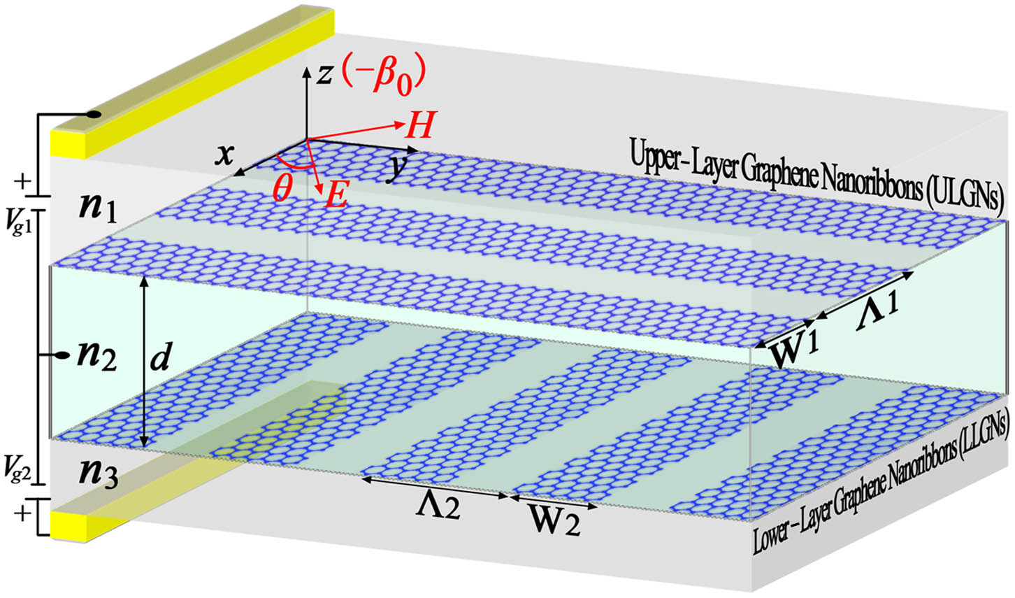
The system under study is schematically depicted in Fig. 1. Two layers of periodic GNRs are placed parallel to the plane and separated by a distance . The upper-layer GNRs (ULGNRs) are periodic in the direction and extend infinitely along the direction, whereas the lower-layer GNRs (LLGNRs) are rotated by 90° relative to the ULGNRs. The geometric parameters, defined as shown in Fig. 1, are fixed as follows unless otherwise specified: , , and . The dielectric constants of the three subdivided regions are set to , , and . For simplicity, the GNRs are assumed to be embedded in a homogeneous dielectric with , unless otherwise specified. This approximation is chosen to elucidate the fundamental principles of PIT and to emphasize the coupling mechanism between the GNRs; it has been used in many theoretical studies [39–44] because its simplicity does not affect any of the fundamental conclusions. It can be trivially extended to a practical situation such as graphene sheets separated by a Si or spacer with permittivity and further covered by two independent ion-gel gates with dielectric constant [10,11,28,45]. Technologically, realization of the proposed PIT system is experimentally feasible using the well-developed patterning techniques recently used to prepare layered GNRs with similar, and even smaller, geometrical values [28,45,46].
Figure 1.Schematic of the PIT system. Two layers of periodic GNRs with crossed ribbon directions are placed parallel to the plane; the upper and lower layers have ribbon widths and and transverse periods and , respectively. The layers are separated by a distance . The ribbon layers are assumed to be separated by a conductive Si or spacer with refractive index and further covered by two independent ion-gel gates with refractive indices . The Fermi levels of the GNRs can be tuned simultaneously by applying two independent bias voltages between the two top gold gates and the conductive spacer. A normally incident plane wave with wave number and polarization angle with respect to the axis strikes the surface of the periodically structured graphene system.
The proposed structure is simulated by the finite-difference time-domain (FDTD) method using Lumerical FDTD Solutions. In our simulations, periodic boundary conditions are imposed along both the and axes, and perfectly matched layers are applied on the top and bottom of the unit cell to absorb all the light approaching the boundaries. Broadband plane waves are incident from the direction at the polarization angle with respect to the axis and are normal to the graphene surface throughout our analyses. The mesh size inside the graphene layer is set to 0.2 nm along the axis and 2 nm along the and axes, and the mesh size gradually increases outside the graphene layer. To ensure the validity of the simulation, a simulation time of 5000 fs and the highest mesh accuracy are set in the mode. Because the GNRs are tens of nanometers wide, it is necessary to mention quantum versus classical effects. The optical responses of nanostructured graphene described by first-principles calculations and classical local electromagnetic theory have been shown to be in good agreement, provided that the size of the graphene topography exceeds 10 nm [39,43]. Thus, in our work, we use classical descriptions to study the optical response of the GNRs while reasonably neglecting any quantum finite-size and edge effects (zigzag and armchair configurations). The graphene film is modeled by the random-phase approximation (RPA) in our numerical simulations and also in theoretical analyses [5,9]. Within the RPA, the optical conductivity of doped graphene can be approximately written as a Drude-like expression in the spectral range of interest: [10,45,47]. Here, is the chemical potential of graphene, which is determined by the carrier concentration, [where is the measured dc mobility, is the reduced Planck constant, and is the Fermi velocity] and which can be tuned by electrical gating [10,11,28,45]. Further, is the angular frequency of the incident light, and is the carrier relaxation time, which satisfies the relationship . Unless otherwise specified, we fix at 0.6 eV, which is a relatively conservative value compared with the highest experimentally feasible values () [48,49]. The permittivity of graphene is modeled by an anisotropic dielectric tensor considering its single-atom thickness. Its component is set to on the basis of the dielectric constant of graphite, and the in-plane components are [10,50,51], where is the vacuum permittivity, and is the thickness of graphene. The value of is reasonable here owing to the large difference between the thickness and the width of the graphene. The simulated results show excellent agreement for , 0.5, and 1 nm, provided that the mesh is sufficiently fine. We emphasize that in this work we focus exclusively on the optical properties of the layered system; thus, we assume that the GNRs are homogeneously doped in each layer and have uniform distributions of the Fermi energy over their surfaces.
3. RESULTS AND DISCUSSION
A. PIT with Single Transparency Window
In recent years, the nanophotonics community has focused on GNRs as one of the most important building blocks in the nanostructured graphene family because they are relatively easy to obtain experimentally and they can confine optical fields below the diffraction limit by supporting localized plasmons (mainly Fabry–Pérot-like standing wave resonances) [11,47,51] or propagating plasmons [40,52]. These resonances depend critically on the ribbon width and optical properties, the control of which at the atomic scale is a major challenge. In this section, we exploit the properties of GNRs and the plasmonic coupling between them to demonstrate an extraordinary PIT effect.
In Fig. 2, we show the results of electromagnetic simulations of the setup shown in Fig. 1 under excitation by a normally incident plane wave with (that is, with the electronic field polarized perpendicular to the ULGNRs). Two transmission dips (absorption peaks) are clearly visible at 4.55 and 3.71 µm. The one at the longer resonant wavelength is dominant for transmission as low as 3.89% (or absorption reaching 30.71%), whereas that at the shorter resonant wavelength is characterized by a transmission dip of 8.86% (or an absorption peak of 41.68%), indicating that these two modes are very strongly coupled under external incidence, as shown in Figs. 2(a) and 2(b). In Fig. 2(c), we also calculated the delay times at the two sharp notches, which reach and , respectively, indicating fast light propagation in the system. Note that, because the fast light effects occur at the transmission minima, the better fast light performance comes at the cost of lower light transmission through the system, making the fast light effect meaningless.
Figure 2.(a) Transmission and (b) absorption spectra of the structure with normal incidence and polarization angle . Solid green curves and symbols represent the analytical and numerical results, respectively. (c) Transmission phase (left vertical axis) and delay time (right vertical axis) of the spectra shown in (a) and (b).
To understand the physical mechanisms behind this PIT, we first analyze the system with only the ULGNRs. Figure 3(a) shows the results of numerical simulations of transmission with only the ULGNRs (upper panel) and only the LLGNRs (lower panel). It can be concluded that plasmon oscillations can be strongly excited when the incident wave is polarized perpendicular to the transverse ribbon direction. Under this condition, the GNRs operate in the bright mode. Plasmons cannot be excited when the polarization of the incident wave is parallel to the GNRs because of a strong momentum mismatch. In this case, they can be treated as the dark mode. Excitation of plasmons in GNRs can be understood by considering the induced charge density or the induced dipole/multipole moment [see Appendix A, Eqs. (A14) and (A17)]. As these parameters are both proportional to the external incidence , they will reach their maximum and minimum when they are perpendicular and parallel to the GNRs, respectively. Note that these conclusions are in agreement with experimental results [11,53,54]. For the two-layer system, because the ribbons are oriented perpendicular to each other, the case with only LLGNRs is the same as that with only the upper layer, except for a polarization angle difference of 90°. It is indeed this difference that causes the different excitation efficiencies of the two layers; because the incident waves are polarized perpendicular to the ULGNRs and parallel to the LLGNRs (), plasmons in the ULGNRs can be excited directly and therefore represent the bright mode. Conversely, the LLGNRs represent the dark mode but can be induced by the bright mode. This bright–dark mode interaction causes PIT.
Figure 3.Two-dimensional plots of normal-incidence transmission showing the wavelength versus the polarization angle for the proposed system with (a) only ULGNRs (upper panel) and only LLGNRs (lower panel) and (b) two-layer GNRs. The left inset in (a) shows the component of the incoming beam at 4.26 µm with only ULGNRs; the right inset plots the transmission dips for only ULGNRs (dark line) and only LLGNRs (red line) versus the polarization angle . The inset in (b) depicts the transmission dips of the QAM and QSM versus the polarization angle . Spatial distributions of (c)–(e), (i)–(k) the electric field and (f)–(h), (l)–(n) the corresponding component of the (c)–(h) QAMs and (i)–(n) QSMs at polarization angles of (c), (f), (i), (l) 0°, (d), (g), (j), (m) 45°, and (e), (h), (k), (n) 90°. Plus and minus signs denote the oscillating surface charges; darker color represents higher charge density.
This coupling mechanism can be ruled out by examining the electric field distributions and the corresponding components at the two transmission dips, which are plotted in Figs. 3(c), 3(f), 3(i), and 3(l). According to the spatial distributions of the components parallel to the plane, the mode at 4.55 µm shows an antiphase resonance within the two layers. This mode is called the quasi-asymmetric mode (QAM) because it results from the out-of-plane nature of the structure. The mode at 3.71 µm shows the in-phase resonance, which is called the quasi-symmetric mode (QSM). In addition, these figures clearly show the structure of these modes. The components of the electric field show a dipole mode resonance characterized by a phase shift in each period [51]; thus, these two modes are the only fundamental modes. Strong enhancement of the electromagnetic fields is observed for both of these modes, as their absorption exceeds 30%. Interestingly, the polarity of the ULGNRs is the same as that for only ULGNRs in these modes, as shown in the inset of Fig. 3(a). In contrast, for the LLGNRs, the polarity of the induced fields has the opposite distribution in the two modes, as shown in Figs. 3(f) and 3(l). Indeed, the polarity inversion defines two forbidden transitions at separate resonances while giving rise to an allowed transition window that is shifted in the transmission spectrum relative to the original case with only ULGNRs [Fig. 2(a)].
In addition to the introduction of bright and dark modes, an excellent feature of such a layered system is its insensitivity to the polarization direction. Figure 3(b) shows that both the transmission dips and the resonant positions in the PIT spectra are totally insensitive to the polarization angle. This can be understood by considering the induced fields in the two layers. As described by Eq. (C1) in Appendix C, the resonant moment (where or 2 is the layer order) in each GNR is proportional to the external field. For the ULGNRs, this resonant moment is a cosine function, whereas for the LLGNRs, it is a sine function. Owing to the distinctive geometric arrangement of the two graphene layers, when the polarization angle changes, regardless of whether the excitation efficiency has been enhanced or weakened in the upper layer, it will be compensated for by the lower layer, making the system polarization insensitive.
To demonstrate the mechanism more clearly, we plot the electric field distributions at polarization angles of 0°, 45°, and 90° in Figs. 3(c)–3(n). We first note that when , the field distribution is just the reverse of that when . This is because the LLGNRs operate as the bright mode, whereas the ULGNRs operate as the dark mode. In particular, when , both the ULGNRs and LLGNRs can be directly excited at the same position [Fig. 3(a)], where the two layers will interact further with each other. Considering that the coupling between the two graphene layers [see Appendix B, Eq. (B3)] contributes to both the intralayer and interlayer interactions, and that the geometrical parameters are the same in the two layers (e.g., , and ), the interactions between them, and , are equivalent. Further, the only supported modes in the two layers will be excited at the same position [11,40]. Thus, the plasmon waves in each ribbon can be thought of as a combination of directly excited waves and induced ones, as clearly shown in Figs. 3(f)–3(h) for the QAM and in Figs. 3(l)–3(n) for the QSM. That is, at both the QAM and QSM resonances, both the ULGNRs and LLGNRs operate as the bright and dark modes simultaneously at the same position, which is vastly different from the usual PIT behavior, where the bright and dark modes can be generated only in different resonators under one particular polarization direction of the incident waves [16,17,22–28,33].
By further tracking the induced polarizability in each ribbon from the moment and the coupling between them using the PWFs, the transmission , reflection , and absorbance coefficients of the th graphene layer can then be obtained using Eqs. (C2)–(C4) in Appendix C. Then, the total transmission, reflection, and absorption efficiencies of the dielectric–graphene hybrid multilayer system can be calculated using the TMM with Eqs. (D3)–(D5) in Appendix D. We obtain excellent agreement between the numerical and analytical calculations, as illustrated in Figs. 2(a) and 2(b), where the dots are calculated from Maxwell’s equations using the FDTD method, and the solid curves correspond to the analytical models using the combined PWFs and TMM.
Because strong coupling causes the induced transparency effect, anything that strongly affects the coupling pathway will serve as a tuning parameter for the transparency window. To identify such parameters, we first conducted parametric studies with by varying the ribbon widths of the bright mode () and the dark mode () from 20 to 100 nm, as shown in Figs. 4(a) and 4(b), respectively. Because the ULGNRs represent the bright mode, a change in their width directly affects the excitation efficiency of the entire system. For example, when is small enough, the coupling with the external field is weak, and therefore the system becomes transparent. In particular, when (that is, the ULGNRs become a graphene sheet), the two graphene layers are all dark, and the PIT disappears. In contrast, variation of the dark mode () can modulate only the window distance and the linewidth of the QAM and QSM but cannot eliminate the high coupling efficiency. Even when the LLGNRs become an integrated carbon sheet (), the two induced modes are still fully coupled, as in a two-dimensional case reported earlier [34]. On the other hand, as we fix the ribbon widths and then tune the interlayer separation , the coupling strength decreases monotonically [see Appendix B, Eq. (B3)], increasing the transparency of the QSM and further resulting in an asymmetric transmission line shape, as shown in Fig. 4(c). At the same time, the two modes approach each other. At a sufficiently large distance (e.g., ), as expected, the two layers are almost uncoupled because the lower layer is well beyond the decay length of the evanescent diffraction orders of the upper layer [Fig. 8(d)]. As a result, the symmetric mode is extinguished (that is, it becomes dark), and only the antisymmetric mode remains.
Figure 4.Transmission maps of the system at a polarization angle of 0° showing the incident wavelength versus (a) the ribbon width of the ULGNRs, (b) the ribbon width of the LLGNRs, and (c) the distance between the two layers.
In addition to their geometrical structures, an intriguing property of graphene-based plasmonic devices (as compared with metal-based structures) is their ultrabroad and active tunability, which is achieved by electrostatic gating techniques. This property allows the transmission window of the designed PIT systems to be dynamically modulated to different positions by electrically changing the Fermi energy of graphene without reoptimizing the physical structure [10,11]. By employing an electrolytic gate, the Fermi energy level has been experimentally increased to 0.8 eV [48] or even higher (1.2 eV) [49] after a high bias voltage was applied by a field-effect transistor structure; thus, in this paper, we conservatively assume that the Fermi energy can be continuously tuned from 0.2 to 0.6 eV. Practically, as shown in Fig. 1, this dynamic tunability can be achieved by applying individual voltages to the gates on both sides, which allows the carrier concentration in each graphene sheet to be uniformly and independently controlled. The simulated transmission map shown in Fig. 5(a) confirms the broadband and dynamic tuning with changes in the Fermi level. For a given ribbon width and coupling distance, the plasmon wavelengths are described by a scaling behavior, [40,47,51], as indicated by the lines with symbols in the inset of this figure. This universal relation is characteristic of two-dimensional electron gases [11] and will be advantageous in the design of active graphene optoelectronic devices.
Figure 5.(a) Two-dimensional transmission map of the system plotted as the wavelength versus the Fermi level . The inset, which has the same coordinates as the main plot, compares the analytically calculated resonant wavelengths (lines) and the numerical solutions of the system (symbols). (b) Refractive index sensitivity of the QAM and QSM as a function of polarization angle .
In addition to their dynamic tunability by the doping concentration, the induced QAM and QSM are extremely sensitive to the local dielectric environment, as confirmed by the PWFs in Eqs. (B7) and (C2)–(C4) in Appendices B and C, so they can be effectively used to design a refractive index sensor. As shown in Fig. 5(b), we calculate the sensitivities of the two modes for fully angular polarizations when the layered GNRs are immersed in media characterized by different values of the refractive index between 1.0 and 1.1. To quantify the performance of the system, we define the parameter sensitivity as , which specifies the resonance wavelength shift per refractive index unit (RIU). We observe that the QAM yields a shift of 4.31 μm/RIU, whereas the QSM shows a smaller shift of 3.42 μm/RIU. These values are larger than those found in other studies [16,55–57]. In particular, we note that these two values are completely independent of the polarization angle, unlike the directionally constrained structures that have been reported [16,43,55–57]. To the best of our knowledge, this is the first report on a completely polarization-insensitive refractive index sensor that does not use any rotationally symmetric structures (such as disks). This complete polarization angle insensitivity will greatly advance practical sensing applications.
B. PIT with Two Transparency Windows
In the previous section, we demonstrated that by designing two crossed GNR layers, obvious PIT with a single transparency window is obtained, and we further analyzed it numerically and theoretically. Because the geometrical parameters of the two layers are identical, the equivalent and complementary coupling behavior yields total insensitivity to the polarization angle. However, for different polarization directions, the induced transparency can be the result of either one-way bright–dark mode interactions (when the polarization angle is perpendicular or parallel to the GNRs) or hybridized coupling of bidirectional bright–bright and bright–dark modes (when the polarization angle is inclined with respect to the GNRs). It is well known that the optical properties of a system rely fundamentally on the symmetry of its constituent parts. This is particularly true of plasmonic systems, where the observation of exotic optical effects such as PIT requires the coupling of modes that emerge only in systems with nontrivial broken symmetries. In this section, this concept will be illustrated by using graphene layers with unequal widths. The inequivalent interactions in systems with a solid upper layer and systems with a solid lower layer result in PIT with two transparency windows.
Figure 6(a) maps the transmission as the incident wavelength versus the polarization angle when and . This figure indicates that, in contrast to that of the system with equal ribbon widths [Fig. 3(b)], the transmission is highly polarization dependent. To show this more clearly, we selected the spectra for , 45°, and 90°, as plotted in Fig. 6(b). When the polarization is perpendicular or parallel to any layer (0° and 90°, respectively), two transmission dips and only one transmission window appear at different positions. Interestingly, when the polarization is inclined with respect to the ribbons, there are four well-defined forbidden transitions at separate resonances. Two allowed transition windows appear in the transmission spectrum and are shifted relative to those of the two original systems with only ULGNRs and LLGNRs [Fig. 6(b)].
Figure 6.(a) Transmission map of the symmetry-broken PIT system with and plotted as the wavelength versus the polarization angle . (b) Transmission spectra of the system for polarization angles of 0°, 45°, and 90°. Green circles represent the ULGNR-only case with , and blue circles represent the LLGNR-only case with . The red solid curves are obtained using the analytical model, and the numerical results are presented as black circles. (c)−(f) Spatial distributions of the electric fields at the positions of the transmission dips extracted from (b) for . Plus and minus signs indicate the oscillating surface charges.
To reveal the physical concepts underlying the PIT with two transparency windows, the near-field intensity distributions in the graphene plane are computed and are plotted in Figs. 6(c)–6(f) for the four transmission dips labeled in Fig. 6(b) for . There are two reasons for the four forbidden transitions in the spectrum. First, as the fundamental components excite surface plasmon waves, GNRs support size-dependent plasmonic resonances. The resonance wavelength can be described as a function of the width, [40,47,51]; thus, the supported bright and dark modes in the two layers will occur at different positions. Second, the differing ribbon widths of the two layers result in unequal coupling strengths and [see Appendix B, Eq. (B3)].
The nature of the charge density of these four plasmon resonances indicates that they are all hybrid fundamental dipole–dipole coupled modes. The two modes labeled c and e in Fig. 6(b) originate from direct excitation of the LLGNRs and their further coupling with the dark mode (ULGNRs). On the basis of the arrangement of their dipole moments [Figs. 6(c) and 6(e)], these two modes are called the first-order QAM1 (FOQAM1) and first-order QSM1 (FOQSM1), respectively. The other two modes, labeled d and f in Fig. 6(b), are the result of direct excitation of the ULGNRs and their further interactions with the dark mode (LLGNRs). Similarly, as shown in Figs. 6(d) and 6(f), these two modes are called the first-order QAM2 (FOQAM2) and first-order QSM2 (FOQSM2), respectively. That is, the two graphene layers operate as both the bright and dark modes simultaneously in this double PIT effect. This coupling mechanism is very different from those that arise from one bright mode coupled with two dark modes [58,59]. In addition, to further confirm that the multiple transmission windows are indeed two PIT windows, we calculated the corresponding group delay times and found a maximum value of , which implies that the system with different ribbon widths exhibits fast light behavior. Again, by applying PWFs combined with the TMM (see Appendices A–D), we find excellent agreement between the numerical and analytical calculations, as shown in Fig. 6(b).
4. CONCLUSIONS
We demonstrate numerically and theoretically that PIT is achievable using two crossed GNR layers. Each GNR layer can operate as either the bright mode, the dark mode, or both the bright and dark modes simultaneously when the polarization is perpendicular/parallel or tilted with respect to the GNRs, respectively. Specifically, when the two layers are designed with equal (unequal) ribbon widths, the geometrically induced symmetric (asymmetric) plasmon excitations and interlayer coupling produce single-window (double-window) PIT with high polarization independence (dependence). Finally, the proposed concepts are analyzed using PWFs combined with the TMM. In all cases, the agreement between the analytical and numerical results is nearly perfect. The proposed designs and developed methods are essential to understanding recent reports and the fundamental coupling mechanisms of PIT and could advance practical applications of graphene-based plasmon devices, including optical modulators and plasmonic sensors.
APPENDIX A. EIGENMODE RESONANCES AND PWFs IN A SINGLE GNR
The GNRs examined in this work have widths much smaller than the resonant wavelengths associated with their plasmon frequencies. Thus, we can safely describe their optical response in the electrostatic limit. We begin our analyses with the case of a single graphene island. Following the formalism from the low-dimensional structures presented in Refs. [42–44], we intend to find the electric field produced by a planar GNR in response to a normal-incidence field arriving from the direction, . The optical electric field can be formulated as a self-consistent equation [10,43,60]: where is the average permittivity of the materials surrounding the graphene plane. The integral is the induced scalar potential, and the expression in square brackets represents the induced charge density, which can be further written in terms of the current by using the two-dimensional, local, space- and frequency-dependent Drude model of the anisotropic graphene conductivity [50]. We further assume that for homogeneously doped graphene, the conductivity can be separated as , where is an occupation function with a value of 1 when the in-plane position vector lies within the graphene plane and 0 elsewhere (a vanishing positive number in practice). Here, we introduce the dimensionless coordinate vector , where is the ribbon width. We now define [44]Equation (A1) can be recast as where , and is a symmetric matrix that is invariant under exchange of its arguments: . This means that is a real, symmetric operator that can produce a complete set of real eigenvalues and orthonormalized eigenvectors for the th ordered mode that satisfy [42,44] such that the eigenmodes satisfy the complete orthogonality condition and the closure relation where is the identity matrix in the subspace of the quasi-static electric field modes.
Using the above eigenmodes, the solution of Eq. (A3) can be expressed in terms of these eigenmodes as [42] with the expansion coefficients given by where, according to the closure relation, we have which allows us to write the induced field as Here it is convenient to define the PWFs associated with mode as which describes the induced charge density profiles associated with confined plasmonic mode . From Eqs. (A5) and (A6), the PWFs are found to meet the orthonormality condition Using the continuity of the electric field, we can rewrite the induced charge density as By integrating Eq. (A11) by parts, the expansion coefficients can be reduced to where which is a parameter that acts as the moment of the corresponding mode. Therefore, the induced charge density allows us to calculate the induced dipole/multipole moment as Comparing the definition of the polarizability, , and inserting Eq. (A14) into Eq. (A17), the polarizability can be expressed as a tensor, which allows us to calculate the transmission properties of a GNR from the knowledge of the corresponding PWFs.
To test the above theory, the PWFs of the first four lowest-order plasmon modes (; see labels) in a single GNR along the transverse ribbon direction are shown in Fig. 7(a). The induced charge distributions from the numerical simulations are represented by symbols, and the analytical results from the PWFs are represented by solid curves. In all cases, the agreement is nearly perfect.
Figure 7.(a) PWFs of the four lowest-ordered plasmon modes (; see labels) in a graphene ribbon along the transverse ribbon direction. The symbols represent the numerical model, and the solid curves represent analytical functions. (b) Electric field components of the first four modes (; see labels). Note that the color bars are the same. The numerical results in this figure were obtained at a fixed wavelength (4547.4 nm) using eigenmode analyses with a ribbon width of 50 nm and Fermi level of graphene of 0.6 eV.
To rule out the role of excitation behavior of different-order mode resonances and to understand the physical mechanisms controlling the plasmonic coupling in PIT, we compute the transmission spectrum of a single GNR under normal incidence, as shown in Fig. 8(a). A cross-sectional view of the component of the electric field profile associated with the wavelengths with strongest transmission (corresponding to modes , 3, 5, 7) is shown in Fig. 8(b). We observe a standing wave pattern for each mode with increasing mode order for decreasing wavelength. A comparison of Fig. 8(b) with Fig. 7(b) reveals that only odd-ordered modes with odd-symmetric phases at the ribbon boundaries are generated. This is because only plasmonic modes with odd multiples of half-wavelengths can couple with normally incident light, as this produces an effective charge dipole that creates the necessary restoring force for collective oscillating waves. The lack of even-ordered modes can be explained as follows. Owing to the symmetry of the GNR around the axis, the induced charge density of the even-ordered modes has even symmetry; thus, the mode moments [see Eq. (A16)] under a normally incident field, which has been shown both theoretically and experimentally [53,61]. Therefore, in the following analyses, only (with ) ordered mode resonances are considered.
Figure 8.(a) Simulated transmission (red line) and absorption (blue line) spectra of a single GNR, where the ribbon width and graphene parameters are set to the same values as in Fig. 7. (b) Electric field components of the first four modes (, 3, 5, and 7; see labels) show excitation of only the odd-ordered modes at normal incidence. Note the differences between the color bars. (c) and (d) Spatial distributions of the normally excited electric fields for the first six lowest-ordered modes in the directions parallel and perpendicular to the graphene surface, respectively.
We now consider plasmonic coupling among multiple GNRs. We denote the th ribbon in the th layer (with or 2) by and the center position by . The other parameters of the th ribbon are the conductivity , eigenvalue , eigenmode , PWF , and mode moment for plasmon modes . The corresponding position vectors are defined as , where is the in-plane position vector of the related th ribbon, and is the width of the th ribbon. Note that is a global variable that runs over the surfaces of all of the ribbons and is normalized within each of the corresponding ribbon widths. Therefore, the induced charge density can be decomposed as a sum of the contributions from each ribbon in a self-consistent form [43,44] with the expansion coefficients where , and . Further, describes the coupling between plasmon modes and in two GNRs and that are separated by a vector , where integration over and is restricted to the surfaces of each nanoribbon. Note that the above equations take into account both the interlayer and intralayer coupling among the lower and upper graphene layers. After Eq. (B3) is solved, the induced moment on ribbon can be expressed as Then, it is convenient to rewrite Eq. (B2) in terms of these moments as where is the th order modes coupling, whereas describes the ribbon polarizability per unit length of the th ribbon.
APPENDIX C. DIPOLE–DIPOLE MODEL OF PERIODIC GNRs
The spatial distributions of the normally excited plasmonic fields for the six lowest-ordered modes are shown in Figs. 8(c) and 8(d). Field singularities are avoided by using rounded corners at the edges, where the radius of curvature corresponds to half of the graphene thickness. The field is maximum at the edge boundaries of the GNR for all modes, and the field intensities of higher-order modes are orders of magnitude smaller than those of lower-ordered modes. This is understandable because the absorption of higher-order modes is much lower than that of lower-order ones. Away from the graphene surfaces, the surface plasmon polariton field decays more rapidly with increasing distance from the graphene sheet. The natural spatial distributions of the induced fields are the dominant factor responsible for the coupling between the GNRs.
In Figs. 9(a) and 9(b), we show the coupling behavior calculated using Eq. (B3) for different coupling distances and different mode orders, respectively. Because the ribbon widths are the same and the periods are fixed at the same values in both layers, the induced charge density should be independent of and dependent mainly on the mode order . Further, because the charge densities are orthonormal [see Eq. (A13)], we need to consider only the coupling between modes with the same order.
Figure 9.Coupling strengths (a) for different coupling distances of the mode and (b) for different mode orders in the nearest-neighbor ribbon. The left panels show intralayer () and interlayer () coupling, whereas the right panels show the sums of the coupling strengths.
We first consider coupling with different coupling distances for the fixed lowest mode, . As Fig. 9(a) shows, the coupling strength decreases rapidly with increasing interaction spacing, and the strength of interlayer coupling is much smaller than that of intralayer coupling. However, we find that even if we consider the tenth-nearest-neighbor interactions, the summed contribution of all these couplings is improved by just 4.7% when compared with the result for only the first-nearest-neighbor interactions. For the interactions of modes of different orders, the sum of the coupling of the first six lowest-ordered modes added only 0.7% to the coupling of the lowest mode, . That is, the most prominent coupling corresponds to the fundamental plasmon mode, and the higher-order resonances become increasingly weaker. The small contributions from both the high-ordered modes and widely separated ribbons can be explained by the spatial distributions of the induced evanescent fields; they decay rapidly with increasing distance from the graphene surface, as shown in Figs. 8(c) and 8(d). These results suggest that, for the parameters considered in our analyses, long-distance and high-order mode interactions can be reasonably ignored, and it is enough to consider the leading contribution of just the first-nearest-neighbor interactions in the lowest dipole mode.
Therefore, for simplicity, we study only the optical response of the PIT system within a spectral region dominated by the lowest-ordered dipole–dipole model () within the nearest-neighbor ribbons. Again, owing to the uniform ribbon width and period in the two layers, and further considering the geometric symmetry of the system, we find that the total resonant moment, the corresponding polarizability, and the coupling strength should be independent of . Thus, , , and , and we can solve Eq. (B5) as where is a matrix of elements. For the case considered in this appendix, only the nearest-neighbor coupling for the mode is considered. Therefore, we have , where represents the intralayer dipole–dipole interaction, which in the long-wavelength limit () reduces to [41], and describes the interlayer dipole–dipole interaction [see Eq. (B3)]. Note that even though this equation is independent of the geometric parameters of a structure, the polarizability and coupling strengths are still related to the incident angle.
Ultimately, for periodic GNR arrays, the transmission () and reflection () coefficients of the th graphene layer are then obtained [41,62]: where , and ; the superscripts represent the effective refractive index of the dielectric above or below the graphene layer. Finally, the absorbance of the layer is
APPENDIX D. TRANSFER MATRIX METHOD IN THE LAYERED SYSTEM
To demonstrate the simulated results, the TMM is used to theoretically calculate the light propagation in the layered system [63]. Considering the ultrathin nature of the graphene sheet, for simplicity, the structure shown in Fig. 1 is modeled as a planar three-layer system with three subdivided layers and two interfaces [dielectric 1 ()–graphene interface 1–dielectric 2 ()–graphene interface 2–dielectric 3 (); see Fig. 1]. According to Maxwell’s equations and with appropriate boundary conditions, the field amplitudes above ( and ) and below ( and ) the th interface () can be expressed as where the superscripts denote the transmitted/reflected fields, and represent the field amplitudes above/below the graphene interface. We state that in the long-wavelength limit (), the propagation phase in the sandwiched dielectric layer is negligible. Therefore, the field amplitudes of the input and output waves in the system can be obtained from the transfer equation here , and .
When incident light impinges only from the top dielectric layer (that is, ) and propagates downward in the negative- direction, the reflection , transmission , and absorption of the multilayer PIT system can be respectively described as The accuracy of the models using the PWFs combined with the TMM is illustrated in Figs. 2(a), 2(b), and 6(b). The dots are calculated from Maxwell’s equations using the FDTD method. The solid curves correspond to the analytical models using the PWFs combined with the TMM. We obtain excellent agreement between the numerical and analytical calculations.