
Tiesheng Wu, Xueyu Wang, Huixian Zhang, Yiying Wang, Weiping Cao, Yiping Wang. Ultra-Broadband Perfect Absorber Based on Multilayered Zr/SiO2 Film[J]. Acta Optica Sinica, 2021, 41(5): 0516001
- Acta Optica Sinica
- Vol. 41, Issue 5, 0516001 (2021)
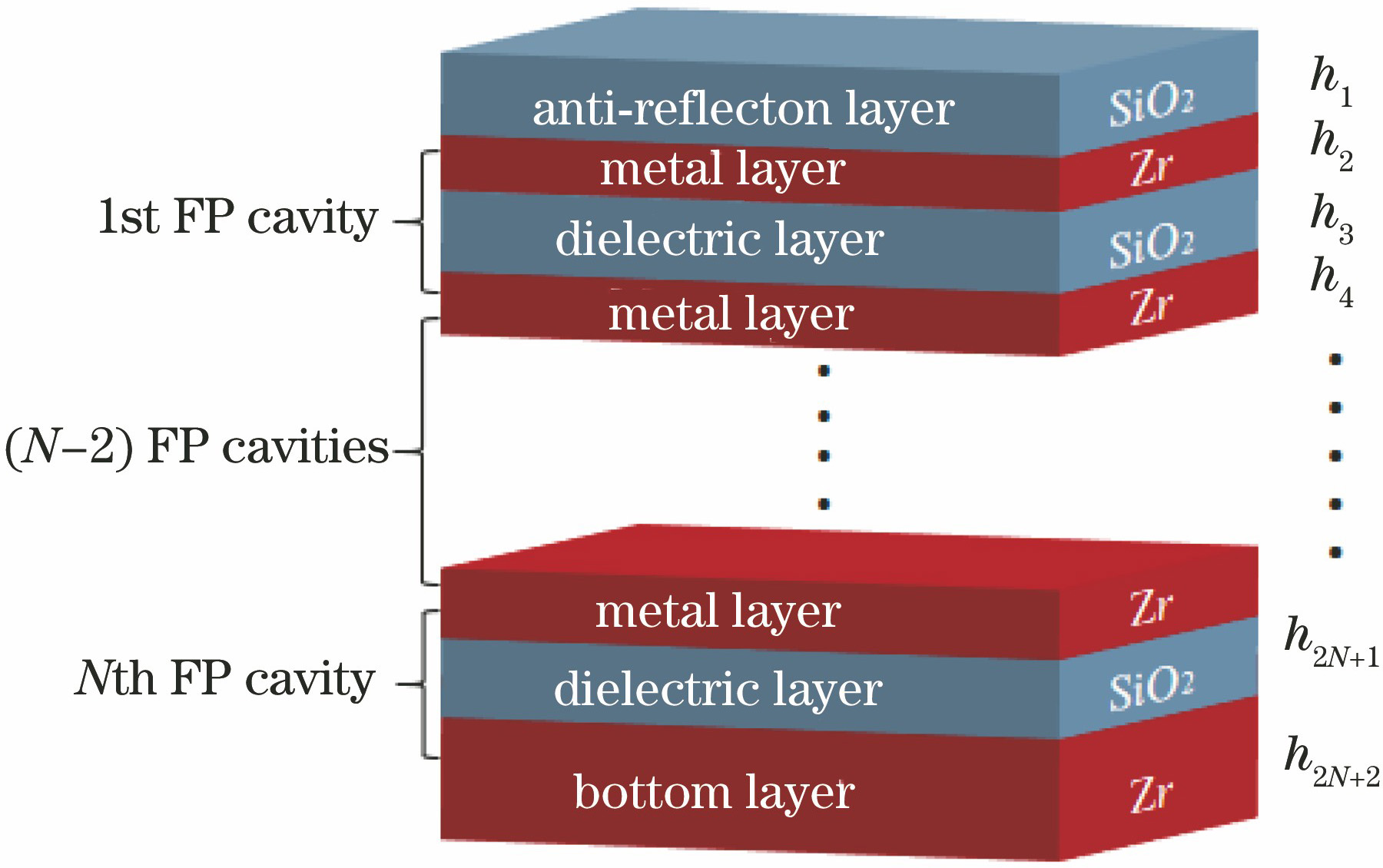
Fig. 1. Structural diagram of multilayered planar metal/dielectric ultra-broadband absorber
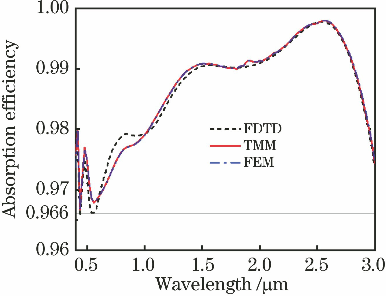
Fig. 2. Absorption spectra of 10-layered Zr/SiO2 absorber
Fig. 3. Optical properties of absorbers for different metal films. (a) Absorption spectra; (b) normalized impedance
Fig. 4. Relationship between each physical variable and wavelength. (a) Electric field intensity; (b) absorption intensity; (c) absorption efficiency of each metal layer
Fig. 5. Absorption spectra of absorbers with different film layer thicknesses. (a) h1; (b) h2; (c) h3; (d) h4; (e) h5; (f) h6; (g) h7; (h) h8
Fig. 6. Absorption spectra of absorbers with different film layer numbers
Fig. 7. Relationship between light absorption efficiency and incident angle under different polarization conditions. (a) TE polarization; (b) TM polarization
Fig. 8. Relationship between temperature rise and each parameter. (a) Temperature rise versus luminous intensity for different incident wavelengths; (b) temperature rise versus incident wavelength for different luminous intensities
Fig. 9. Absorption spectrum of absorber, normalized solar radiation spectrum and normalized radiation spectra of black body at different temperatures
|
Table 1. Structural parameters for realizing highest average absorption efficiency of absorbers with different layer numbers in range of 0.4--3.0 μm
|
Table 2. Relationship between optimal average absorption efficiency and layer number for each wavelength rangeunit: %
|
Table 3.

Set citation alerts for the article
Please enter your email address
© Copyright 2018-2021 | Chinese Laser Press. All Rights Reserved 沪ICP备15018463号-20