
Yu-Zhe LIN, Jeremy A. MASSENGALE, Wen-Xiang HUANG, Rui-Qing YANG, Tetsuya D. MISHIMA, Michael B. SANTOS. Examination of the durability of interband cascade lasers against structural variations[J]. Journal of Infrared and Millimeter Waves, 2020, 39(2): 137
- Journal of Infrared and Millimeter Waves
- Vol. 39, Issue 2, 137 (2020)
Abstract
Keywords
Introduction
After more than 20 years of efforts since the original proposal of interband cascade (IC) lasers (ICLs) in 1994 at the 7th Inter. Conf. on Superlattices, Microstructures and Microdevices[
Incomplete understandings or even misconceptions have also affected the development of ICLs. For example, one may perceive that the design and growth of ICLs are difficult due to their complexities, and consequently look for non-cascade approaches[
1 Device design, growth, and fabrication
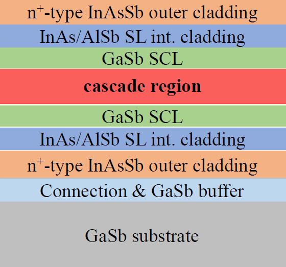
The ICL structure was designed based on an improved waveguide configuration, which was initially used successfully in InAs-based ICLs[
![]()
Figure 1.Schematic drawing of layer structure for GaSb-based ICLs
Following the same ICL design, wafers M368 and M370 were grown by solid-source molecular beam epitaxy (MBE) on 2-inch diameter GaSb (100) substrates. The structural parameters were characterized by using a Philips MRD high resolution x-ray diffraction (XRD) system.
![]()
Figure 2.X-ray diffraction data for wafers M368 (top) and M370 (middle) and a corresponding simulation (bottom) of an ω-2θ scan around the (004) reflection for the GaSb substrate. The scans are offset for clarity
The wide central peak, shown between Δθ of ±400 arcsec in the inset to
The two wafers were processed into deep-etched broad-area (150- and 100-µm-wide) mesa stripe lasers by contact photolithography and wet chemical etching. Wafer M370 was cleaved into two pieces that were processed separately. Devices for wafer M370 will be labeled with #1 and #2 for the first- and second-time processes, respectively. The processed wafers were cleaved into laser bars with a length of 1.5 mm and the facets were left uncoated. The laser bars were mounted epilayer side up on copper heat sinks with indium solder and placed on the cold finger of a cryostat for measurements in cw and pulsed modes. In pulsed measurements, the applied current pulse width was 1 μs at a repetition rate of 5 kHz.
2 Device performance and discussion
Broad-area devices made from M368 and M370 lased in cw mode at temperatures up to 220 K (at 3.685 μm) and 228 K (at 3.893 μm as shown by the inset to
![]()
Figure 3.Current-voltage-light characteristics for a 150-μm-wide device from M370 in cw operation. The inset is the cw lasing spectrum from a 100-μm-wide device at a various heat-sink temperature
At 80 K, the lasing wavelength varied from 3.45 to 3.53 μm for devices at different locations in wafer M370, while it ranged from 3.30 to 3.41 μm for devices from wafer M368, implying nonuniformities in the structural parameters across each wafer and between the two wafers. A device from a location near the wafer edge had a lasing wavelength somewhat shorter than a device near the center of the wafer. With an increase in temperature, the lasing wavelengths became longer as shown in Figs. 3 and 4. For example, at 300 K, two 150-μm-wide devices from M370 lased in pulsed mode at 3.87 μm and 3.98 μm (top inset to
![]()
Figure 4.Lasing wavelength of broad-area ICLs. Inset: pulsed lasing spectra (M368 and M370) at 300 K
The lasing wavelengths of these ICLs at 300 K are significantly shorter than the targeted value of 4.6 μm. This is qualitatively consistent with the x-ray diffraction data that indicates that the cascade stages are about 6% thinner than the design value for the two wafers. However, thinner layers in the active QW regions may cause about 200 nm blue shifts due to the higher energy levels, but do not completely account for the significant blue shifts of the lasing wavelengths (> 600 nm in M370 and 700 nm in M368). Other factors that may affect the energy levels of QWs and thus lasing wavelengths include possible variations in interface compositions, incorporation of residual As or Sb, and uneven flux fluctuations from different cells during MBE growth. The lasing wavelengths of the ICLs from wafer M368 were somewhat shorter than from wafer M370, but increased with temperature at a slightly faster rate (2.54 nm/K vs. 2.22 nm/K in pulsed operation) as shown in
Since the two ICL wafers had substantial structural deviations from the design, as reflected from the lasing wavelengths, significant device performance degradation (or even nonfunction) were expected. Nevertheless, devices made from these wafers still performed very well. In pulsed operation, two devices from M368 lased at temperatures up to 355 K near 3.96 μm (lower inset to
![]()
Figure 5.Threshold current density vs temperature for devices from wafers M368 and M370. Symbols and colors are consistent with those in Fig.4. Two insets are pulsed lasing spectra for three devices near their thresholds
Their threshold current densities as a function of temperature are shown in
3 Summary and concluding remarks
In summary, the effects of structural variations on ICL device performance were investigated by examining the characteristics of devices made from two wafers with layer thicknesses and compositions that unintentionally deviated considerably from the design. We showed that although the lasing wavelengths of the ICLs were significantly shifted from the targeted value, the device performance was still very good in terms of threshold current density and operating temperature. This is partially attributed to the advantages and flexibility of ICLs based on interband transitions with a much longer lifetime than the intraband relaxation time via the fast phonon scattering. Also, we demonstrated that the improved plasmon waveguide configuration[
References
[1] R Q YANG. Infrared laser based on intersubband transitions in quantum wells. Superlattices and Microstructures, 17, 77-83(1995).
[2] R Q YANG. in
[3] I Vurgaftman, R Weih, M Kamp. Interband cascade lasers. : Appl. Phys, 48, 123001(2015).
[4] I E Trofimov, C L Canedy, C S Kim. Interband cascade lasers with long lifetimes. Appl. Optics, 54, 9441-9445(2015).
[5] L LI, H YE, Y C JIANG. MBE-grown long-wavelength interband cascade lasers on InAs substrates. J. Crystal Growth, 425, 369-372(2015).
[6] R Q YANG, L LI, W X HUANG. InAs-based Interband Cascade Lasers. IEEE J. Selected Topics Quantum Electronics, 25, 1200108(2019).
[7] J Koeth, R Weih, J Scheuermanna. Infrared Remote Sensing and Instrumentation XXV, San Diego, United States, 10403, 1040308(2017).
[8] L Shterengas, G Kipshidze, T Hosoda. Cascade Pumping of 1.9-3.3 µm Type-I Quantum Well GaSb-based Diode Lasers. IEEE Journal of Selected Topics in Quantum Electronics, 23, 1-8(2017).
[9] J Faist, F Capasso, D L Sivco. Quantum cascade laser. Science, 264, 553-556(1994).
[10] D Jung, S R Bank, M L Lee. Next generation mid-infrared sources. . Opt, 19, 123001(2017).
[11] R Q YANG, S S PEI. Novel type-II quantum cascade lasers. J. Appl. Phys, 79, 8197-8203(1996).
[12] L LI, Y JIANG, H YE. Low-threshold InAs-based interband cascade lasers operating at high temperatures. Appl. Phys. Lett, 106, 251102(2015).
[13] L Esaki, L L CHANG, E E Mendez. 532. Phys, 20, L529(1981).
[14] J R Meyer, C A Hoffman, F J Bartoli. Type-II quantum-well lasers for the mid-wavelength infrared. Appl. Phys. Lett, 67, 757-759(1995).
[15] R Q YANG, L LI, L H Zhao.
[16] C L Canedy, M V Warren, C D Merritt. Quantum Sensing and Nano Electronics and Photonics XIV, San Francisco, United States, 10111, 101110G(2017).
[17] A Schade, S Höfling. Infrared Remote Sensing and Instrumentation XXV, San Diego, United States, 10403, 1040305(2017).
[18] 18YANGR Q. Mid-infrared interband cascade lasers based on type-II heterostructures [J]. Microelectronics J., 1999, 30(10): 1043-1056;and references therein.
[19] 19YANGR Q, BradshawJ L, BrunoJ D, et al. Mid-infrared type-II interband cascade lasers [J]. IEEE J. Quantum Electron., 2002, 38(6): 559-568;and references therein.

Set citation alerts for the article
Please enter your email address
© Copyright 2018-2021 | Chinese Laser Press. All Rights Reserved 沪ICP备15018463号-20