Abstract
The self-heating effect severely limits device performance and reliability. Although some studies have revealed the heat distribution of β-Ga2O3 MOSFETs under biases, those devices all have small areas and have difficulty reflecting practical conditions. This work demonstrated a multi-finger β-Ga2O3 MOSFET with a maximum drain current of 0.5 A. Electrical characteristics were measured, and the heat dissipation of the device was investigated through infrared images. The relationship between device temperature and time/bias is analyzed.1. Introduction
Ultra-wide bandgap β-Ga2O3 is a promising candidate for advanced high-power applications owing to its outstanding material properties, including a large bandgap of ~4.8 eV, a high critical breakdown field of 8 MV/cm and a large Baliga’s figure of merit of 3444[1, 2]. Low-cost and scalable melting growth techniques such as edge-defined film-fed growth (EFG)[3] and Czochralski[4] methods give advantages to β-Ga2O3 over other wide bandgap materials such as SiC, GaN and diamond. Among these material properties of β-Ga2O3, low thermal conductivity (11–27 W/(m·K) at 300 K) can cause a severe self-heating effect (SHE) and affect device reliability and stability[5].
β-Ga2O3 power metal–oxide–semiconductor field-effect transistors (MOSFETs) have been investigated since 2012[6] and have achieved remarkable results[7-11]. Constructive methods have been proposed to minimize the SHE of β-Ga2O3 MOSFETs[12, 13], such as the ion-cutting technique[14], transfer to a foreign substrate[15, 16] and structural design[17]. Novel measurements have been used to characterize the transient temperature distribution of β-Ga2O3 MOSFETs[18]. Most reports on β-Ga2O3-based MOSFETs have focused on pursuing high PFOMs and exploring novel structures, yet large-area structures are needed to sustain a high on-state current for practical applications. For large-area structures, SHE will be more serious compared with small devices because of the smaller surface area-to-volume ratio, which is worth investigating. The main challenge of fabricating high performance large-area β-Ga2O3 transistor is the inhomogeneity of material growth and instable process flow. There have been reports that multi-finger β-Ga2O3 MOSFETs are capable of delivering 300 V switching transients with voltage slopes reach up to 65 V/ns[19], showing great potential. Nonetheless, the electrical and thermal properties of this technology remain to be thoroughly explored. In this work, we fabricated a multi-fingers β-Ga2O3 MOSFET with output current reach to 0.5 A. DC characteristics have been studied. We have employed optical thermography to investigate the impact of the self-heating effect on the multi-finger β-Ga2O3 MOSFET.
2. Experiment
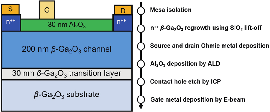
A semi-insulating Fe-doped (010) β-Ga2O3 bulk substrate was used in this work. A β-Ga2O3 film with a concentration of ~2 × 1017 cm–3 was grown on the substrate by MOCVD. Before film growth, a 30-min wafer carrier bake was performed for cleaning at 860 °C. Details of growth and doping can be found in our previous report. Fig. 1 shows the cross-sectional schematic of the fabricated β-Ga2O3 MOSFET. The fabrication process started with mesa isolation was performed by BCl3/Ar inductively coupled plasma (ICP) dry etching. Then, 300 nm of SiO2 was grown by plasma-enhanced chemical vapor deposition (PECVD) at 300 °C, and source/drain areas were exposed by buffered oxide etching (BOE) for regrowth of the heavily doped ohmic contact region by MOCVD. After that, SiO2 was fully removed by hydrofluoric acid solution for over 30 min. The Ti/Au (20/180 nm) metal stack was then deposited by electron beam evaporation and subjected to rapid thermal annealing at 470 °C for 1 min in a nitrogen atmosphere. Thereafter, 30 nm thick Al2O3 was deposited as the gate dielectric layer by atomic layer deposition (ALD) at 250 °C, and pad regions were opened by removing Al2O3 using ICP etching. Finally, Ni/Au (20/80 nm) gate metal was deposited by electron beam evaporation. Small-area transistors with a gate width (Wg) of 10 µm, a gate-to-source distance (Lgs) of 2 µm, a gate-to-drain distance (Lgd) of 7 µm and a gate length (Lg) of 2 µm were fabricated to evaluate the device properties. The device temperature distribution was characterized by a Fluke TiX580 infrared thermal imaging camera.

Figure 1.(Color online) Cross-sectional schematic of the β-Ga2O3 MOSFET and its process flow.
3. Results and discussion
The DC characteristics of the small-area transistor were determined by a Keysight B1500A semiconductor device analyzer. Fig. 2(a) shows the transfer characteristics of the small-area MOSFET. A threshold voltage Vth = –11 V, subthreshold swing SS = 190 mV/dec and an on/off ratio Ion/Ioff > 108 were extracted. Fig. 2(b) illustrates the output characteristics of the small-area MOSFET. The saturation drain–source current Ids = 63 mA/mm and on-state resistance Ron = 20.2 Ω·mm were obtained. Fig. 2(c) shows the off-state characteristics of the small-area device, which was carried out by a Keysight B1505A power device analyzer. Gate bias was kept at –15 V during the test. A three-terminal breakdown voltage of 400 V was obtained.
Figure 2.(Color online) DC (a) transfer and (b) output characteristics of small-area MOSFET. (c) Three terminal leakage current under the off-state.
Figs. 3(a) and 3(b) give an optical microscope image of a multi-finger β-Ga2O3 MOSFET and its layout. The multi-finger MOSFET featured a finger-to finger distance of 20 µm, which is composed of Lgs = 4 µm, Lg = 4 µm and Lgd = 12 µm. Each finger has a width of 20 µm. The large-area transistor showed an on-state current of 0.5 A and an on-resistance of 13 Ω, as shown in Fig. 3(d). The different threshold voltages between large-area and small-area devices can be ascribed to epitaxial β-Ga2O3 film. The current and voltage level is still lagging behind the small-area device due to uniformity issues in material growth and the device fabrication process. Upon the establishment of mature material growth and fabrication process, the inherent advantages of the material can be fully demonstrated.
Figure 3.(Color online) (a) Optical microscope image and (b) layout of a multi-finger β-Ga2O3 MOSFET. (c) Transfer and (d) output characteristics of multi-finger MOSFET.
The temperature distribution images measured by the infrared camera are shown in Figs. 4(a)–4(d). The gate electrode was kept floating during the test. According to the results, the heat was mainly generated in the β-Ga2O3 channel between the source and drain and then mainly dissipated through the metals, which explains why the metal possessed a lower temperature during the tests. This phenomenon became more obvious in the thermal equilibrium state (see Fig. 5(a)). The maximum temperature in the β-Ga2O3 channel almost reached 250 °C under an applied voltage of 8 V, showing the severe self-heating effect of the large-area transistor. The primary reason for the comparatively reduced temperature of the metal pad is primarily ascribed to its superior conductivity in comparison to β-Ga2O3. It is worth noting that the reflectivity and emissivity of the metal surface could potentially impact the precision of temperature measurement. To alleviate SHE, effective cooling mechanisms are necessary to regulate the SHE, including the implementation of high-thermal-conductivity carrier wafers[15] for top-side or flip-chip integration[20], as well as the utilization of heat sinks[12].
Figure 4.(Color online) Temperature distribution images with biased time of (a) 0 s, (b) 10 s, (c) 20 s and (d) 50 s. The drain bias was set as 2 V. (e) Time dependence of the maximum temperature in the β-Ga2O3 channel with different drain voltages.
Figure 5.(Color online) Thermal equilibrium state: (a) temperature distribution image with a drain voltage of 8 V and (b) maximum temperature in the β-Ga2O3 channel versus applied drain voltage.
4. Conclusion
In summary, we present a multi-finger β-Ga2O3 MOSFET with a saturation current over 0.5 A. The self-heating effect was investigated by infrared images. The generation and dissipation actions were analyzed. This work provides a better understanding of the self-heating effect of large-area β-Ga2O3 MOSFETs and is significant for high-power applications.
References
[1] M Higashiwaki, K Sasaki, H Murakami et al. Recent progress in Ga2O3 power devices. Semicond Sci Technol, 31, 034001(2016).
[2] H Dong, H W Xue, Q M He et al. Progress of power field effect transistor based on ultra-wide bandgap Ga2O3 semiconductor material. J Semicond, 40, 011802(2019).
[3] A Kuramata, K Koshi, S Watanabe et al. High-quality β-Ga2O3 single crystals grown by edge-defined film-fed growth. Jpn J Appl Phys, 55, 1202A2(2016).
[4] Y Tomm, P Reiche, D Klimm et al. Czochralski grown Ga2O3 crystals. J Cryst Growth, 220, 510(2000).
[5] Y T Yu, X Q Xiang, X Z Zhou et al. Device topological thermal management of β-Ga2O3 Schottky barrier diodes. Chin Phys B, 30, 067302(2021).
[6] M Higashiwaki, K Sasaki, A Kuramata et al. Gallium oxide (Ga2O3) metal-semiconductor field-effect transistors on single-crystal β-Ga2O3 (010) substrates. Appl Phys Lett, 100, 013504(2012).
[7] H Y Liu, J N Li, Y J Lv et al. Improved electrical performance of lateral β-Ga2O3 MOSFETs utilizing slanted fin channel structure. Appl Phys Lett, 121, 202101(2022).
[8] A Bhattacharyya, P Ranga, S Roy et al. Multi-kV class β-Ga2O3 MESFETs with a lateral figure of merit up to 355 MW/cm². IEEE Electron Device Lett, 42, 1272(2021).
[9] X Z Zhou, Y J Ma, G W Xu et al. Enhancement-mode β-Ga2O3 U-shaped gate trench vertical MOSFET realized by oxygen annealing. Appl Phys Lett, 121, 223501(2022).
[10] C L Wang, H Zhou, J C Zhang et al. Hysteresis-free and μs-switching of D/E-modes Ga2O3 hetero-junction FETs with the BV2/Ron, sp of 0.74/0.28 GW/cm2. Appl Phys Lett, 120, 112101(2022).
[11] X Zhou, Q Liu, W Hao et al. Normally-off β-Ga2O3 power heterojunction fieldeffect-transistor realized by p-NiO and recessed gate. IEEE 26th Int Symp Power Semiconductor Devices IC’s (ISPSD)(2022).
[12] S Kim, Y W Zhang, C Yuan et al. Thermal management of β-Ga2O3 current aperture vertical electron transistors. IEEE Trans Compon, Packag Manufact Technol, 11, 1171(2021).
[13] B Chatterjee, K Zeng, C D Nordquist et al. Device-level thermal management of gallium oxide field-effect transistors. IEEE Trans Compon Packag Manuf Technol, 9, 2352(2019).
[14] W H Xu, Y B Wang, T G You et al. First demonstration of waferscale heterogeneous integration of Ga2O3 MOSFETs on SiC and Si substrates by ion-cutting process. 2019 IEEE International Electron Devices Meeting (IEDM), 12(2019).
[15] J Noh, S Alajlouni, M J Tadjer et al. High performance β-Ga2O3 nano-membrane field effect transistors on a high thermal conductivity diamond substrate. IEEE J Electron Devices, 7, 914(2019).
[16] H Zhou, K Maize, J Noh et al. Thermodynamic studies of Ga2O3 nanomembrane field-effect transistors on a sapphire substrate. ACS Omega, 2, 7723(2017).
[17] B Chatterjee, W Li, K Nomoto et al. Thermal design of multi-fin Ga2O3 vertical transistors. Appl Phys Lett, 119, 103502(2021).
[18] N Kumar, D Vaca, C Joishi et al. Ultrafast thermoreflectance imaging and electrothermal modeling of β-Ga2O3 MESFETs. IEEE Electron Device Lett, 41, 641(2020).
[19] J Böcker, K Tetzner, S Heucke et al. Dispersion effects in on-state resistance of lateral Ga2O3 MOSFETs at 300 V switching. Electon Lett, 56, 838(2020).
[20] H H Gong, F Zhou, X X Yu et al. 70-μm-body Ga2O3 Schottky barrier diode with 1.48 K/W thermal resistance, 59 A surge current and 98.9% conversion efficiency. IEEE Electron Device Lett, 43, 773(2022).