• Chinese Optics Letters
  • Vol. 20, Issue 6, 062501 (2022)
Yuxuan Li1, Xiaobin Liu1, Xuetong Li1, Lanxuan Zhang1, Baisong Chen1, Zihao Zhi1, Xueyan Li1, Guowei Zhang2、3, Peng Ye2、3, Guanzhong Huang2、3, Deyong He2、3, Wei Chen2、3, Fengli Gao1, Pengfei Guo4, Xianshu Luo4, Guoqiang Lo4, and Junfeng Song1、5、*
Author Affiliations
  • 1State Key Laboratory of Integrated Optoelectronics, College of Electronic Science and Engineering, Jilin University, Changchun 130012, China
  • 2CAS Key Laboratory of Quantum Information, University of Science and Technology of China, Hefei 230026, China
  • 3CAS Center for Excellence in Quantum Information and Quantum Physics, University of Science and Technology of China, Hefei 230026, China
  • 4Advanced Micro Foundry Pte Ltd., Singapore 117685, Singapore
  • 5Peng Cheng Laboratory, Shenzhen 518000, China
  • show less
    DOI: 10.3788/COL202220.062501 Cite this Article Set citation alerts
    Yuxuan Li, Xiaobin Liu, Xuetong Li, Lanxuan Zhang, Baisong Chen, Zihao Zhi, Xueyan Li, Guowei Zhang, Peng Ye, Guanzhong Huang, Deyong He, Wei Chen, Fengli Gao, Pengfei Guo, Xianshu Luo, Guoqiang Lo, Junfeng Song. Germanium-on-silicon avalanche photodiode for 1550 nm weak light signal detection at room temperature[J]. Chinese Optics Letters, 2022, 20(6): 062501 Copy Citation Text show less

    Abstract

    To optimize the dark current characteristic and detection efficiency of the 1550 nm weak light signal at room temperature, this work proposes a Ge-on-Si avalanche photodiode (APD) in Geiger mode, which could operate at 300 K. This lateral separate absorption charge multiplication APD shows a low breakdown voltage (Vbr) in Geiger mode of -7.42 V and low dark current of 0.096 nA at unity gain voltage (VGain=1 = -7.03 V). Combined with an RF amplifier module and counter, the detection system demonstrates a low dark count rate (DCR) of 1.1×10⁶ counts per second and high detection efficiency η of 7.8% for 1550 nm weak coherent pulse detection at 300 K. The APD reported in this work weakens the dependence of the weak optical signal recognition on the low environment temperature and makes single-chip integration of the single-photon level detection system possible.

    1. Introduction

    Since the development of weak optical signal recognition technology, the research community has made many important discoveries in optical information fields, such as optical communication, artificial intelligence, and Internet of Things[1]. A photomultiplier tube (PMT)[2,3] with a vacuum tube structure was first, to the best of our knowledge, used for weak light detection, which has the disadvantages of complicated fabrication process, high cost, and large power consumption with relatively large form factor. With the advancement of semiconductor technology, semiconductor-based solid state photosensitive detectors with high integration and stability, such as p-i-n photodetector[46] and avalanche photodiode (APD)[713], have been gradually replacing the PMT in many applications. Due to the inner avalanche multiplication mechanism, APD in the Geiger mode can be widely used as a single-photon avalanche diode (SPAD) in weak light detection applications such as quantum information, machine vision, and more recently LiDAR for optical sensing[1418].

    At present, commercial InGaAs/InP APD in the Geiger mode has been widely used in weak light detection with a wavelength of 1550 nm[19,20]. However, due to the incompatibility with Si-based integrated circuits, these discrete products are usually bulky and cumbersome with limited portability. In contrast, with the industrial-grade production capability of the Si CMOS fabrication platform, Ge-on-Si APD has advantage of lower cost than the InGaAs/InP device and can make up an efficient integrated optical system with other Si-photonics elements, which improves the overall stability of the detection system[21]. However, because of the lattice mismatch of 4% between Ge and Si, there are lots of dislocation defects in the Ge buffer layer, which contributes extra dark count noise under the electric field and severely deteriorates the sensitivity of the APD[22]. To suppress the dark count rate (DCR) of devices, existing SPADs need to work at temperatures lower than 200 K[2328]. However, the refrigeration equipment increases the system cost and power consumption. Furthermore, the narrow bandgap of Ge material increases as the environment temperature drops, which degrades the absorption efficiency of Ge at 1550 nm. Therefore, these devices operating at low temperature can only detect weak coherent pulse with wavelength of 1310 nm effectively. To address the need of weak coherent pulse detection at 1550 nm, this work proposes a waveguide integrated Ge-on-Si APD with a lateral separate absorption charge multiplication (SACM) structure. With unity multiplication gain voltage of 7.03V applied, the dark current of the APD is lower than 0.1 nA at 300 K. With the pulse average photon number of one, the DCR and η of the APD detection system at excess voltage (Vex) of 20% × Vbr are 1.1×10⁶counts per second (cps) and 7.8%, respectively, which makes a 1550 nm weak light detection system operating at room temperature possible.

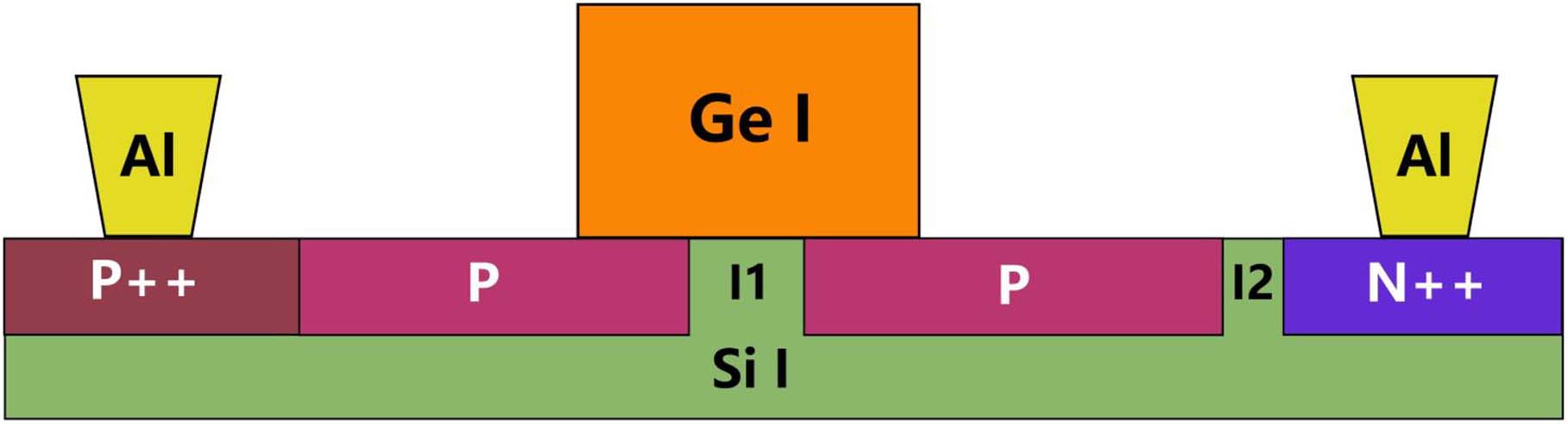
    2. Device Design and Fabrication

    The APDs were fabricated in a standard Si-photonics platform. The structure diagram of the device is shown in Fig. 1. Phosphorus and boron implantation in the 220 nm top Si substrate was performed to form N and P-type regions. The heavily doped N++- and P++-regions are used to form ohmic contact with Al electrodes. The P region with doping concentration of 1019cm3 is used to adjust the electric field of two intrinsic regions I1 and I2. The widths of intrinsic regions I1 and I2 are 0.5 µm and 0.4 µm, respectively. Subsequently, a Ge absorption layer of 20μm(length)×2.0μm(width)×0.5μm(height) was epitaxially grown on the Si substrate.

    Structure diagram of the lateral SACM Ge-on-Si APD.

    Figure 1.Structure diagram of the lateral SACM Ge-on-Si APD.

    As depicted in Fig. 2, When the APD operates at a low reverse bias, the P region located in the middle of two intrinsic regions is not depleted, resulting in the electric field unable to extend to the I1 region effectively, and the energy band of electrons in the I1 region is lower than that in the P-type region. Therefore, the electrons in the I1 region hardly overcome the barrier and cannot transit to the I2 region successfully, which inhibits the dark current effectively. With a high bias applied, the electric field in the I2 region is high enough to induce the avalanche of the device. At the same time, the P region is fully depleted, and the electric field in the I1 region is also improved, resulting in the energy band in the P region being lower than the one in the I1 region, and the free electrons effectively can move to the avalanche region for multiplication. At the same time, the electric field in the I1 region is much lower than 105V/cm, which can prevent the dislocation defects (recombination centers) at the Ge/Si interface from generating large dark current noise under the action of the high electric field.

    (a) Distribution of valence and conduction bands in the I1 region at -2 V and -9 V (Vex = 20%Vbr). (b) The electric field distribution in the Si substrate at -2 V and -9 V.

    Figure 2.(a) Distribution of valence and conduction bands in the I1 region at -2 V and -9 V (Vex = 20%Vbr). (b) The electric field distribution in the Si substrate at -2 V and -9 V.

    3. Device Performance

    To study the response performance of the device, a 1550 nm CW light signal was guided to an optical grating, and the insertion loss is about 4.35dB/grating. Then, the light was coupled into the absorption layer for photoelectric conversion, and the photo-generated current flowed in the Keysight B1500A for data recording.

    Figure 3(a) shows the I-V curves of the device at the optical power in the range of 30 to 10dBm. As the bias voltage changes from 0 V to 7V, under the action of the barrier effect of the P region, the electric field is confined in the avalanche region and hardly extends to the Ge region. Therefore, the dark current of the APD in the linear mode is only on the 0.1 nA order, which is much better than that of the device with a p-i-n structure. It can be found in Fig. 3(b) that as the reverse bias voltage exceeds 7.42V, the avalanche probability in I1 gradually increases, which means that electron avalanche multiplication occurs. At the same time, the electric field in the I2 region also increases, which gradually extends into the Ge absorption layer and sweeps the photo-generated carriers to the avalanche region for multiplication. Referring to Ref. [25], we define 7.42V as the Vbr in the Geiger mode, which is lower than that of other devices reported. Because the direction of the electric field is not consistent with the distribution direction of the Ge absorption layer and the Si substrate, under the barrier effect of the P-type region, the electric field in the I1 region hardly fills the Ge absorption layer. Therefore, the electrons and holes in the absorption region cannot drift to the Si substrate at the saturation speed, resulting in the 3 dB bandwidth of the device at Vbr being about 64 MHz, which is lower than that of the p-i-n counterpart. The APD with a low working voltage can reduce the energy consumption limit of the detection system, which makes the realization of a large-scale on-chip detection system possible.

    (a) Photo-dark current of the SACM APD. (b) Avalanche probability simulation of the SACM APD.

    Figure 3.(a) Photo-dark current of the SACM APD. (b) Avalanche probability simulation of the SACM APD.

    The VGain=1 can be defined by dividing the simulated photocurrent of device and that of the p-i-n in technology computer aided design software[29]. The VGain=1 is about 7.03V, and the corresponding primary dark current is 0.096 nA at 300 K, which is much lower than that of the other devices with SACM structure[711]. As reported in Ref. [30], the DCR of the APD in Geiger mode is proportional to the primary dark current at VGain=1, which means the lateral APD we designed has the advantage of low DCR in room-temperature weak light detection. At the same time, under the barrier action of the P region, the recombination of photo-generated electrons occurs, causing the responsivity of APD at VGain=1 to be about 33 mA/W. However, with the increase of the electric field in the I1 region, the detection performance of the APD in the Geiger mode can be improved effectively.

    Compared with the existing Ge-on-Si APDs with a wide avalanche region, the avalanche region of the device is only about 0.4 µm, and there is a risk that the APD will be burned down if the excess bias (Vex/Vbr) exceeds 20%. Limited by the low accuracy and high threshold of the time to digital converter (TDC), to record the light and dark signals effectively, the experiment setup shown in Fig. 4 was used[23]. By adding a commercial RF amplifier module, the original electrical signal of the APD can be further amplified. The amplified voltage signal was subsequently imported into the TDC to extract the dark and light count data.

    (a) Setup of the weak light signal detection experiment. The red lines are the optical paths, and the black ones represent the electrical paths. (b) Diagram of the device under test (DUT).

    Figure 4.(a) Setup of the weak light signal detection experiment. The red lines are the optical paths, and the black ones represent the electrical paths. (b) Diagram of the device under test (DUT).

    The DCR of the APD in Geiger mode was studied first. To suppress the after pulsing noise of the device, we used a series of pulses with repetition frequency in the range of 2 kHz to 20 kHz and pulse width τ of 5 ns as the gate signal, which was superimposed with the direct current (DC) signal by using a bias-tee and applied to the device under test (DUT). We calculate the DCR of the detection system at different excess bias by Eq. (1), such that DCR=1τln(1pd),where pd is the dark count probability, calculated by dividing the sum of dark count data in a time histogram over the total number of gate signals. It can be found in Figs. 3(b) and 5(a), as excess bias increases, the avalanche probability of electrons gradually increases, contributing to the increase of DCR. As the excess bias achieves 20%, the DCR of the detection system is about 1.1×10⁶cps, which has the same order of magnitude as the reported Ge-on-Si APDs working in the low-temperature environment. With excess bias at 20%, the DCR of the system was measured as a function of gate pulse repetition frequency. As shown in Fig. 5(b), the DCR of the detection system increases as the repetition rate increases, which is consistent with our prediction and the discovery reported in other researches.

    (a) DCR of the detection system versus excess bias at 300 K. (b) DCR of the detection system versus repetition rate of gate pulse with 20% excess bias applied.

    Figure 5.(a) DCR of the detection system versus excess bias at 300 K. (b) DCR of the detection system versus repetition rate of gate pulse with 20% excess bias applied.

    Next, the optical response performance of the lateral SACM Ge-on-Si APD system for 1550 nm weak coherent pulse was investigated. Considering that the sensitivity of the APD is limited at 300 K, our study focused on the detection efficiency η and noise equivalent power (NEP) for weak coherent pulses with an average photon number of one and full-width at half-maximum (FWHM) of 50 ps, which are calculated by Eqs. (2) and (3)[23,25]: η=1nln(1pd1pc),NEP=hνDE2DCR,where n is the average photon number of weak coherent pulses, and pc is the total count probability in the light condition, calculated by dividing the sum of count data in the time histogram over the total number of gate signals. h and ν are the Planck constant and frequency of the photon, respectively. As shown in Fig. 6, η of the APD detection system rapidly increases as the excess bias increases, which is due to the enhancement of avalanche probability, but the corresponding NEP is inversely proportional to the excess bias. With excess bias of 20%, the detection efficiency η can reach 7.8%, and the NEP is about 2.4×10¹⁵WHz1/2. Since the average photon number of weak coherent pulses is not much less than one, the η we extracted is higher than the theoretical single-photon detection efficiency (SPDE) of the system[25]. However, the η of 7.8% is still a high detection efficiency of the Ge-on-Si APD system for 1550 nm single-photon level signals. The SACM APD can effectively improve the detection distance of Ge-on-Si APD for near-infrared light signals.

    (a) Detection efficiency η of the detection system versus excess bias at 300 K. (b) NEP of the detection system versus excess bias at 300 K.

    Figure 6.(a) Detection efficiency η of the detection system versus excess bias at 300 K. (b) NEP of the detection system versus excess bias at 300 K.

    It has been reported that a balanced detector structure formed by two identical APDs in parallel can improve the sensitivity of detection system[31,32]. By applying the same bias to the APDs and injecting the optical pulse signal into one APD, the output signals of two devices are subtracted, which can suppress the spike noise of the single APD in the gate Geiger mode and improve the detection sensitivity of the detection system. This method can enable the APD system to detect the weak coherent pulse signals with an average photon number lower than one. Meanwhile, the lateral SACM APD and RF amplifier module both work within 10 V bias. This has a great advantage in power consumption and makes the realization of a large-scale single-chip integrated system for 1550 nm weak signal detection at room temperature possible.

    Finally, we investigated the time jitter of the lateral SACM APD in Geiger mode. Because the accuracy of the TDC we used is only 50 ps, which is far larger than those used in other reports, time jitter of the detection system cannot be calculated accurately. Through Gaussian fitting of the time count histogram data recorded by TDC, the FWHM of histogram in Fig. 7 is estimated to be about 585 ps. The corresponding system jitter calculated by Eq. (4) is 248.4 ps, which includes the jitter of the laser, the jitter of the RF amplifier, and the jitter of the Ge-on-Si APD[25]. According to the existing research[24], the jitter of the APD is inversely proportional to the excess bias, and the jitter of the pure Si device is less than 80 ps. Therefore, the large time jitter of the lateral SACM APD is mainly due to the inability of carriers to drift at saturation speed in the Ge absorption layer caused by the weak electric field: σJitterFWHM8×ln(2).

    Histograms of the DUT at 20% excess bias.

    Figure 7.Histograms of the DUT at 20% excess bias.

    4. Conclusion

    To address the problems of the high DCR of the Ge-on-Si APD at 1550 nm and room temperature, this work proposes a Ge-on-Si APD with a lateral SACM structure. By optimizing the concentrations and widths of the doped regions, the electric field in the Ge–Si contact surface of the device is effectively suppressed, and the primary dark current of the APD in linear mode is only about 1010A at 300 K. The breakdown voltage in Geiger mode of the lateral SACM APD is lower than 10 V. With the excess bias of 20%, the DCR of the device is about 1.1×10⁶cps, which weakens the dependence of the weak optical signal recognition on the low environment temperature. For the 1550 nm weak coherent pulse with average photon number of one, the detection efficiency η is 7.8%, and the corresponding NEP is 2.4×10¹⁵W·Hz1/2. The lateral SACM APD makes it possible to realize an integrated single-photon level weak signal detection system working at room temperature and provides hardware support for the handheld devices of LiDAR and other weak near-infrared light detection applications.

    ReferenceTemperature (K)DCR (cps)Wavelength (nm)nη (%)
    [25]805.34×10513100.15.27
    [26]783×105131031
    [27]1251×10513100.0129.4
    This Work3001.1×106155017.8

    Table 1. Detection Performance of Ge-on-Si APD in Geiger Mode

    References

    [1] P. A. Govind. Fiber-Optic Communication Systems(2002).

    [2] A. N. Otte, J. Barral, B. Dolgoshein, J. Hose, M. Teshima. New results from a test of silicon photomultiplier as readout for PET. Nuclear Science Symposium/Medical Imaging Conference, 3738(2004).

    [3] S. Cova, M. Ghioni, I. Rech, F. Zappa. Evolution and prospects for single-photon avalanche diodes and quenching circuits. J. Mod. Opt., 51, 1267(2003).

    [4] H. Chen, P. Verheyen, P. D. Heyn, G. Lepage, J. V. Campenhout. −1 V bias 67 GHz bandwidth Si-contacted germanium waveguide p-i-n photodetector for optical links at 56 Gbps and beyond. Opt. Express, 24, 4622(2016).

    [5] H. -T. Chen, P. Verheyen, M. Rakowski, P. D. Heyn, G. Lepage, J. D. Coster, P. Absil, G. Roelkens, J. V. Campenhout. High-responsivity low-voltage 28-Gb/s Ge p-i-n photodetector with silicon contacts. J. Lightwave Technol., 33, 820(2015).

    [6] Y.-X. Li, X.-B. Liu, X.-T. Li, G.-Q. Lo, J.-F. Song. Surface illuminated interdigitated Ge-on-Si photodetector with high responsivity. Opt. Express, 29, 16346(2021).

    [7] N. Duan, T.-Y. Liow, A. E.-J. Lim, L. Ding, G.-Q. Lo. 310 GHz gain-bandwidth product Ge/Si avalanche photodetector for 1550 nm light detection. Opt. Express, 20,, 11031(2012).

    [8] X. -G. Zeng, Z. -H. Huang, B. -H. Wang, M. Fiorentino, R. G. Beausoleil. Silicon–germanium avalanche photodiodes with direct control of electric field in charge multiplication region. Optica, 6, 772(2019).

    [9] Z.-H. Huang, C. Li, D. Liang, K.-Z Yu, S. Palermo, R. G. Beausoleil. 25 Gbps low-voltage waveguide Si–Ge avalanche photodiode. Optica, 3, 793(2016).

    [10] N. J. D. Martinez, C. T. Derose, R. W. Brock, A. L. Starbuck, A. T. Pomerene, A. L. Lentine, D. C. Trotter, P. S. Davids. High performance waveguide-coupled Ge-on-Si linear mode avalanche photodiodes. Opt. Express, 24, 19072(2016).

    [11] S. A. Srinivasan, M. Berciano, P. S. Lardenois, M. Pantouvaki, J. Van Campenhout. 27 GHz silicon-contacted waveguide-coupled Ge/Si avalanche photodiode. J. Lightwave Technol., 38, 3044(2020).

    [12] Y. Yuan, Z.-H. Huang, X.-G. Zeng, D. Liang, W. V. Sorin, M. Fiorentino, R. G. Beausoleil. High responsivity Si-Ge waveguide avalanche photodiodes enhanced by loop reflector. IEEE J. Sel. Top. Quantum Electron., 28, 3800508(2022).

    [13] D. Benedikovic, L. Virot, G. Aubin, J. M. Hartmann, F. Amar, X. L. Roux, C. A. Ramos, B. Szelag, L. Vivien. Silicon-germanium avalanche receivers with fJ/bit energy consumption. IEEE J. Sel. Top. Quantum Electron., 28, 3802508(2022).

    [14] Y. Li, X. Luo, G. Liang, G. Q. Lo. Demonstration of Ge/Si avalanche photodetector arrays for Lidar application. Optical Fiber Communication Conference, 1(2019).

    [15] D. R. Gozzard, L. E. Roberts, J. T. Spollard, P. G. Sibley, D. A. Shaddock. Fast beam steering with an optical phased array. Opt. Lett., 45, 3793(2020).

    [16] D.-W. Zhuang, L.-X. Zhang, X.-C. Han, Y.-X. Li, F.-L. Gao, J. -F. Song. Omnidirectional beam steering using aperiodic optical phased array with high error margin. Opt. Express, 26, 19154(2018).

    [17] L.-X. Zhang, Y.-Z. Li, Y. Hu, Y.-B. Wang, M. Tao, B.-S. Chen, Q.-X. Na, Y.-X. Li, Z.-H. Zhi, X.-B. Liu, X.-Y. Li, F.-L. Gao, X.-S. Luo, G.-Q. Lo, J.-F. Song. Investigation and demonstration of a high-power handling and large-range steering optical phased array chip. Opt. Express, 29, 29755(2021).

    [18] L.-X. Zhang, Y.-Z. Li, M. Tao, Y.-B. Wang, Y. Hu, B.-S. Chen, Y.-X. Li, G.-Q. Lo, J.-F. Song. Large-scale integrated multi-lines optical phased array chip. IEEE Photonics J., 12, 6601208(2020).

    [19] F. Xu, X. Ma, Q. Zhang, H. -K. Lo, J. -W. Pan. Secure quantum key distribution with realistic devices. Rev. Mod. Phys., 92, 025002(2020).

    [20] G.-W. Zhang, Y.-Y. Ding, W. Chen, F.-X. Wang, P. Ye, G.-Z. Huang, S. Wang, Z.-Q. Yin, J.-M. An, G.-C. Guo, Z.-F. Han. Polarization-insensitive interferometer based on a hybrid integrated planar light-wave circuit. Photonics Res., 9, 2176(2021).

    [21] S. M. Sze, K. K. Ng. Physics of Semiconductor Devices(1981).

    [22] J.-M. Liu. Photonic Devices(2005).

    [23] Z. Lu, Y. Kang, H. Chong, Q. Zhou, H.-D. Liu, J. C. Campbell. Geiger-mode operation of Ge-on-Si avalanche photodiodes. IEEE J. Quantum Electron., 47, 731(2011).

    [24] R. E. Warburton, G. Intermite, M. Myronov, P. Allred, D. R. Leadley, K. Gallacher, D. L. J. M. Lever, Z. Ikonic, R. W. Kelsall, E. H. Ceron, A. P. Knights, G. S. Buller. Ge-on-Si single-photon avalanche diode detectors: design, modeling, fabrication, and characterization at wavelengths 1310 and 1550 nm. IEEE Trans. Electron Devices, 60, 3807(2013).

    [25] J. D. N. Martinez, G. Michael, C. T. Derose, A. L. Starbuck, P. S. Davids. Single photon detection in a waveguide-coupled Ge-on-Si lateral avalanche photodiode. Opt. Express, 25, 16130(2017).

    [26] P. Vines, K. Kuzmenko, J. Kirdoda, D. C. S. Dumas, D. J. Paul, G. S. Buller. High performance planar germanium-on-silicon single-photon avalanche diode detectors. Nat. Commun., 10, 1086(2019).

    [27] L. F. Llin, J. Kirdoda, F. Thorburn, L. L. Huddleston, Z. M. Greener, K. Kuzmenko, P. Vines, D. C. S. Dumas, R. W. Millar, G. S. Buller, D. J. Paul. High sensitivity Ge-on-Si single-photon avalanche diode detectors. Opt. Lett., 45, 6406(2020).

    [28] F. Thorburn, X. Yi, Z. M. Greener, Z. M. Greener, J. Kirdoda, R. W. Millar, L. L. Huddleston, D. J. Paul, G. S. Buller. Ge-on-Si single-photon avalanche diode detectors for short-wave infrared wavelengths. J. Phys. Photonics, 4, 012001(2022).

    [29] S.-Y. Ke, S.-M. Lin, D.-F. Mao, Y.-J. Ye, X.-L. Ji, W. Huang, C. Li, S.-Y. Chen. Design of wafer-bonded structures for near room temperature Geiger-mode operation of germanium on silicon single-photon avalanche photodiode. Appl. Opt., 56, 4646(2017).

    [30] Y. Kang, H. X. Lu, Y.-H. Lo. Dark count probability and quantum efficiency of avalanche photodiodes for single-photon detection. Appl. Phys. Lett., 83, 2955(2003).

    [31] A. Tomita, K. Nakamura. Balanced, gated-mode photon detector for quantum-bit discrimination at 1550 nm. Opt. Lett., 27, 1827(2002).

    [32] C. Park, S. B. Cho, C. Y. Park, S. Baek, S. K. Han. Dual anode single-photon avalanche diode for high-speed and low-noise Geiger-mode operation. Opt. Express, 27, 18201(2019).

    Yuxuan Li, Xiaobin Liu, Xuetong Li, Lanxuan Zhang, Baisong Chen, Zihao Zhi, Xueyan Li, Guowei Zhang, Peng Ye, Guanzhong Huang, Deyong He, Wei Chen, Fengli Gao, Pengfei Guo, Xianshu Luo, Guoqiang Lo, Junfeng Song. Germanium-on-silicon avalanche photodiode for 1550 nm weak light signal detection at room temperature[J]. Chinese Optics Letters, 2022, 20(6): 062501
    Download Citation