• Photonics Research
  • Vol. 9, Issue 6, 1039 (2021)
Yang Li1、†, Haolin Chen2、†, Yanxian Guo1, Kangkang Wang1, Yue Zhang1, Peilin Lan1, Jinhao Guo1, Wen Zhang3, Huiqing Zhong1, Zhouyi Guo1、4, Zhengfei Zhuang1、5, and Zhiming Liu1、*
Author Affiliations
  • 1MOE Key Laboratory of Laser Life Science & SATCM Third Grade Laboratory of Chinese Medicine and Photonics Technology, College of Biophotonics, South China Normal University, Guangzhou 510631, China
  • 2Department of Hematology, The Seventh Affiliated Hospital, Sun Yat-sen University, Shenzhen 518107, China
  • 3Department of Medical Biotechnology, School of Basic Medical Sciences, Guangzhou University of Chinese Medicine, Guangzhou 510006, China
  • 4e-mail: ann@scnu.edu.cn
  • 5e-mail: zhuangzf@scnu.edu.cn
  • show less
    DOI: 10.1364/PRJ.421415 Cite this Article Set citation alerts
    Yang Li, Haolin Chen, Yanxian Guo, Kangkang Wang, Yue Zhang, Peilin Lan, Jinhao Guo, Wen Zhang, Huiqing Zhong, Zhouyi Guo, Zhengfei Zhuang, Zhiming Liu. Lamellar hafnium ditelluride as an ultrasensitive surface-enhanced Raman scattering platform for label-free detection of uric acid[J]. Photonics Research, 2021, 9(6): 1039 Copy Citation Text show less
    Schematic illustration of the SERS detection of uric acid based on HfTe2 nanosheets.
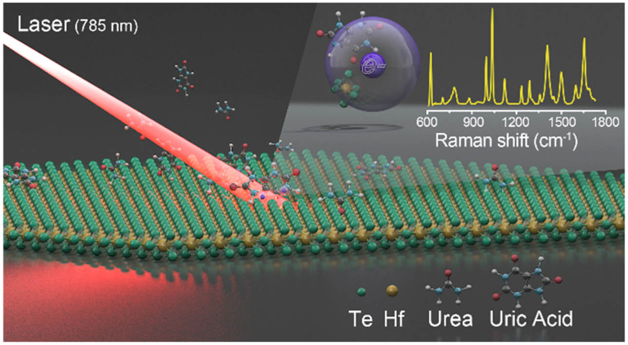
    Fig. 1. Schematic illustration of the SERS detection of uric acid based on HfTe2 nanosheets.
    Synthesis and characterization of HfTe2 nanosheets. (a) Schematic representation of the preparation process of HfTe2 nanosheets. (b)–(c) TEM images of multilayer and few-layered hafnium ditelluride nanomaterials. The inset shows the HRTEM image and SAED pattern, respectively. (d) SEM image of HfTe2 nanosheets. (e) HAADF image and corresponding elemental mapping (Te and Hf) of HfTe2 nanosheets. (f) EDX pattern of HfTe2 nanosheets. (g) AFM image with the corresponding size distribution (inset) and (h) height analysis of HfTe2 nanosheets. (i) Raman spectra of bulk and few-layered HfTe2.
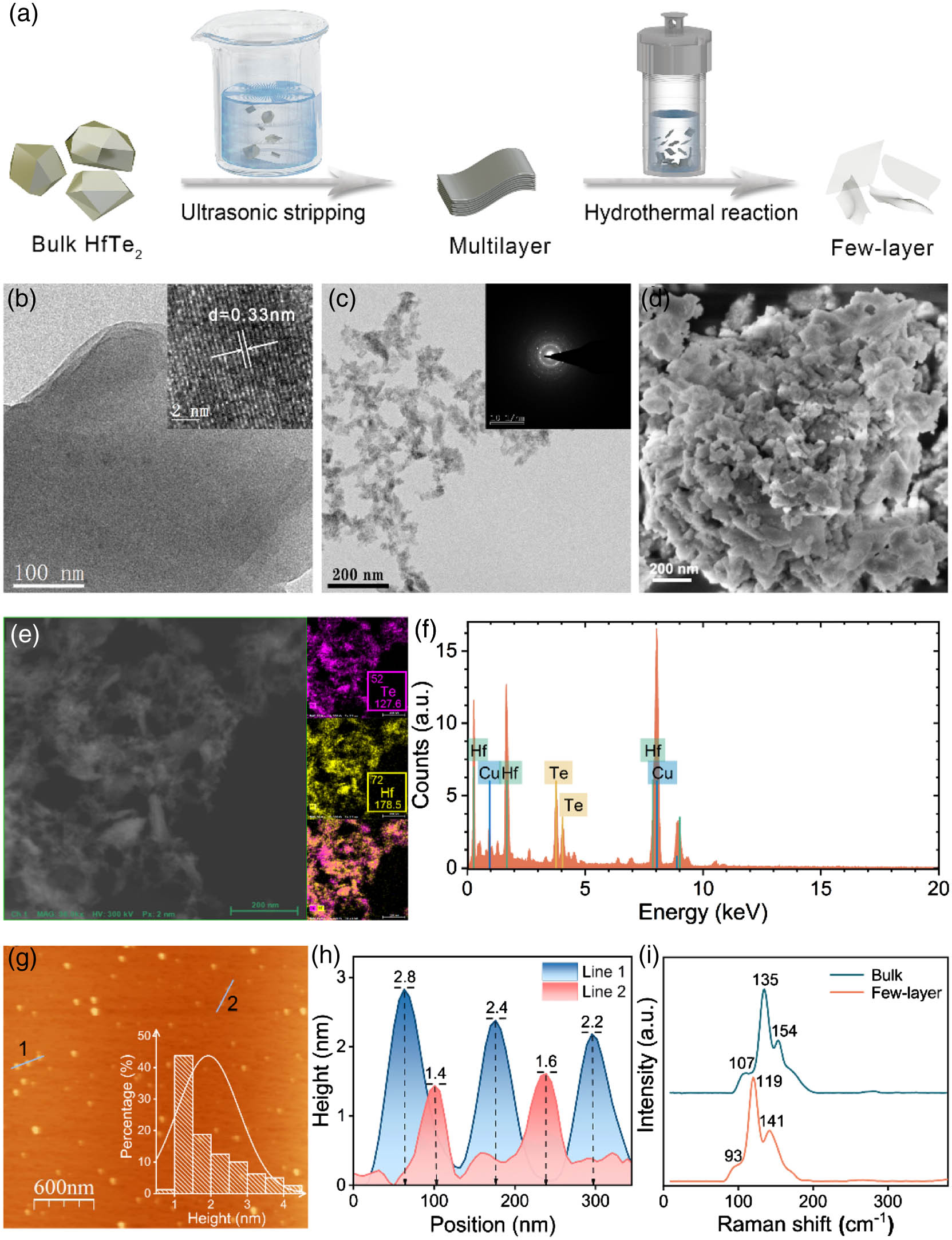
    Fig. 2. Synthesis and characterization of HfTe2 nanosheets. (a) Schematic representation of the preparation process of HfTe2 nanosheets. (b)–(c) TEM images of multilayer and few-layered hafnium ditelluride nanomaterials. The inset shows the HRTEM image and SAED pattern, respectively. (d) SEM image of HfTe2 nanosheets. (e) HAADF image and corresponding elemental mapping (Te and Hf) of HfTe2 nanosheets. (f) EDX pattern of HfTe2 nanosheets. (g) AFM image with the corresponding size distribution (inset) and (h) height analysis of HfTe2 nanosheets. (i) Raman spectra of bulk and few-layered HfTe2.
    Atomic structure of monolayer HfTe2 nanosheet. (a) Left and (b) top views of lattice structures. (c) Unit cell structure of the nanostructures. Green spheres, tellurium atoms; and yellow spheres, hafnium atoms. (d) XRD pattern of HfTe2 nanosheets.
    Fig. 3. Atomic structure of monolayer HfTe2 nanosheet. (a) Left and (b) top views of lattice structures. (c) Unit cell structure of the nanostructures. Green spheres, tellurium atoms; and yellow spheres, hafnium atoms. (d) XRD pattern of HfTe2 nanosheets.
    (a) XPS analysis of HfTe2 nanosheets. The high resolution XPS spectra of Hf 4f in (b) bulk and (c) few-layered HfTe2 sheets. (d) UV-Vis-NIR absorbance spectrum. (e) Typical optical absorption curve of HfTe2 nanosheets, where Eg is estimated to be 4.93 eV. (f) Valence band spectrum of HfTe2 nanosheets, where Evb is calculated to be −4.98 eV.
    Fig. 4. (a) XPS analysis of HfTe2 nanosheets. The high resolution XPS spectra of Hf 4f in (b) bulk and (c) few-layered HfTe2 sheets. (d) UV-Vis-NIR absorbance spectrum. (e) Typical optical absorption curve of HfTe2 nanosheets, where Eg is estimated to be 4.93 eV. (f) Valence band spectrum of HfTe2 nanosheets, where Evb is calculated to be 4.98eV.
    (a) Raw Raman spectra of Rh6G (10−3 M) dye on Si wafer with or without HfTe2 substrate. (b) SERS spectra of different concentrations of Rh6G on HfTe2 substrate. (c) Intensity values of typical Raman peaks in (b). Fitting curve of the inset is the SERS intensity-concentration plot for 1313 cm−1 (R2) band of Rh6G. (d) EF values of five typical Raman peaks of Rh6G at different concentration levels.
    Fig. 5. (a) Raw Raman spectra of Rh6G (103  M) dye on Si wafer with or without HfTe2 substrate. (b) SERS spectra of different concentrations of Rh6G on HfTe2 substrate. (c) Intensity values of typical Raman peaks in (b). Fitting curve of the inset is the SERS intensity-concentration plot for 1313   cm1 (R2) band of Rh6G. (d) EF values of five typical Raman peaks of Rh6G at different concentration levels.
    (a) Cluster of SERS spectra of Rh6G samples randomly collected at 20 sites on the HfTe2 substrate. (b)–(d) SERS intensities of three typical peaks at 1514 cm−1, 1365 cm−1, and 1313 cm−1 in the 20 SERS spectra.
    Fig. 6. (a) Cluster of SERS spectra of Rh6G samples randomly collected at 20 sites on the HfTe2 substrate. (b)–(d) SERS intensities of three typical peaks at 1514  cm1, 1365  cm1, and 1313  cm1 in the 20 SERS spectra.
    (a) SERS image of Rh6G molecules (1514 cm−1) on HfTe2 nanosheets. (b) Contour map of 170 SERS spectra collected from the Raman mapping. (c) Average spectrum (blue line) of the 170 spectral data and the reconstructed spectrum (green line) along the green diagonal line in (b).
    Fig. 7. (a) SERS image of Rh6G molecules (1514  cm1) on HfTe2 nanosheets. (b) Contour map of 170 SERS spectra collected from the Raman mapping. (c) Average spectrum (blue line) of the 170 spectral data and the reconstructed spectrum (green line) along the green diagonal line in (b).
    Schematic diagram of the photo-induced charge transfer process between HfTe2 and Rh6G under 785 nm laser excitation.
    Fig. 8. Schematic diagram of the photo-induced charge transfer process between HfTe2 and Rh6G under 785 nm laser excitation.
    Mean SERS spectra of pure uric acid, urea, and their mixture on HfTe2 nanosheets.
    Fig. 9. Mean SERS spectra of pure uric acid, urea, and their mixture on HfTe2 nanosheets.
    (a) SERS detection of UA at different concentrations on HfTe2 nanosheets. Curves a to j: SERS spectra of UA at 1000, 600, 500, 400, 350, 300, 250, 200, 150, and 100 μM, respectively. Curve k: normal Raman spectrum of UA at 1 mM. (b) Fitting curve of SERS intensity-logarithmic concentration for 1039 cm−1 band of UA. (c) SERS spectra of UA (0.1–0.5 mM) on HfTe2 nanosheets in the presence of 4 mM urea. (d) Calibration curve by plotting the peak intensity ratio (I1039/I1012) as a function of UA concentration. Enlargements of the typical Raman peaks (urea 1012 cm−1, uric acid 1039 cm−1) are shown as insets.
    Fig. 10. (a) SERS detection of UA at different concentrations on HfTe2 nanosheets. Curves a to j: SERS spectra of UA at 1000, 600, 500, 400, 350, 300, 250, 200, 150, and 100 μM, respectively. Curve k: normal Raman spectrum of UA at 1 mM. (b) Fitting curve of SERS intensity-logarithmic concentration for 1039  cm1 band of UA. (c) SERS spectra of UA (0.1–0.5 mM) on HfTe2 nanosheets in the presence of 4 mM urea. (d) Calibration curve by plotting the peak intensity ratio (I1039/I1012) as a function of UA concentration. Enlargements of the typical Raman peaks (urea 1012  cm1, uric acid 1039  cm1) are shown as insets.
    AnalyteRaman Shift (cm1)EF
    Rh6G13131.73×106
    16522.32×106
    MB13021.95×106
    16249.62×105
    CV8251.35×106
    13031.0×106
    MG11763.98×105
    16223.95×105
    Table 1. Calculated Maximum EFs of Typical SERS Peaks of Different Dyes on HfTe2 Substrate
    Yang Li, Haolin Chen, Yanxian Guo, Kangkang Wang, Yue Zhang, Peilin Lan, Jinhao Guo, Wen Zhang, Huiqing Zhong, Zhouyi Guo, Zhengfei Zhuang, Zhiming Liu. Lamellar hafnium ditelluride as an ultrasensitive surface-enhanced Raman scattering platform for label-free detection of uric acid[J]. Photonics Research, 2021, 9(6): 1039
    Download Citation