• Photonics Research
  • Vol. 9, Issue 10, 1892 (2021)
Tianning Zheng1, Bin Wei1、3、*, Fuchuan Lei2、4、*, and Bisong Cao1
Author Affiliations
  • 1Department of Physics, State Key Laboratory Low-Dimensional Quantum Physics, Tsinghua University, Beijing 100084, China
  • 2Department of Microtechnology and Nanoscience, Chalmers University of Technology, SE-41296 Gothenburg, Sweden
  • 3e-mail: weibin@tsinghua.edu.cn
  • 4e-mail: fuchuan@chalmers.se
  • show less
    DOI: 10.1364/PRJ.430185 Cite this Article Set citation alerts
    Tianning Zheng, Bin Wei, Fuchuan Lei, Bisong Cao. Very large group delay in VHF band using coupled high temperature superconducting resonators[J]. Photonics Research, 2021, 9(10): 1892 Copy Citation Text show less
    Design, fabrication, and simulation results. (a) Schematic diagram of the HTS coupled resonator circuit; (b) simulated current density of the HTS coupled resonators’ circuit at the transparent frequency; (c) photograph of the HTS coupled resonator circuit; (d) schematic diagram of fabrication process of the HTS circuit; (e) simulated and theoretical transmission spectra of the HTS coupled resonator circuit; (f) simulated group delay of the HTS coupled resonator circuit. The YBCO film has a conductivity of 1.2×10¹⁴ S/m and a thickness of 600 nm. The substrate is MgO with dimensions of 34 mm×20 mm×0.5 mm, and its relative permittivity is 9.7077. Due to the very low loss of the substrate, the loss tangent during simulation is set as 0, and the loss is equivalent to conductor loss. The depth of the air layer below the top cover is 5 mm. The dimensions in the circuit are as follows: L1=34 mm, L2=20 mm, a1=0.48 mm, a2=0.36 mm, a3=0.08 mm, b1=2.56 mm, s1=0.8 mm, s2=7.2 mm, f=1.20 mm, w1=6.2 mm, and w2=8 mm. The number of turns of each spiral resonator is 12. The linewidth and line spacing are both 0.08 mm in the spiral resonators.
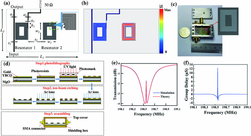
    Fig. 1. Design, fabrication, and simulation results. (a) Schematic diagram of the HTS coupled resonator circuit; (b) simulated current density of the HTS coupled resonators’ circuit at the transparent frequency; (c) photograph of the HTS coupled resonator circuit; (d) schematic diagram of fabrication process of the HTS circuit; (e) simulated and theoretical transmission spectra of the HTS coupled resonator circuit; (f) simulated group delay of the HTS coupled resonator circuit. The YBCO film has a conductivity of 1.2×10¹⁴  S/m and a thickness of 600 nm. The substrate is MgO with dimensions of 34  mm×20  mm×0.5  mm, and its relative permittivity is 9.7077. Due to the very low loss of the substrate, the loss tangent during simulation is set as 0, and the loss is equivalent to conductor loss. The depth of the air layer below the top cover is 5 mm. The dimensions in the circuit are as follows: L1=34  mm, L2=20  mm, a1=0.48  mm, a2=0.36  mm, a3=0.08  mm, b1=2.56  mm, s1=0.8  mm, s2=7.2  mm, f=1.20  mm, w1=6.2  mm, and w2=8  mm. The number of turns of each spiral resonator is 12. The linewidth and line spacing are both 0.08 mm in the spiral resonators.
    Simulation study of EIT, ATS, and Fano resonance of the coupled resonators. (a) Simulated results of transmission spectra as s2 varies, and f is set as 1.02 mm; (b) simulated results of transmission spectra as f varies, and s is set as 7.2 mm; (c) simulated corresponding group delay in (a); (d) simulated corresponding group delay in (b).
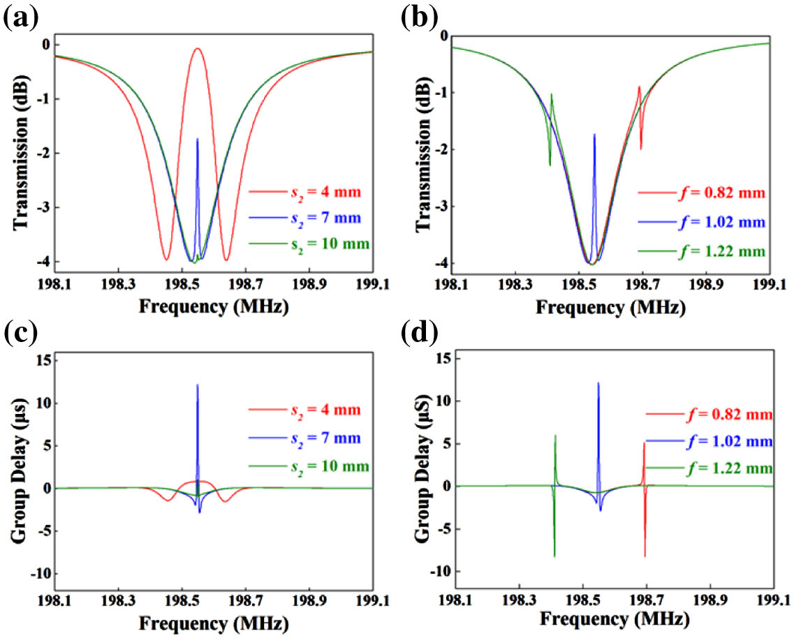
    Fig. 2. Simulation study of EIT, ATS, and Fano resonance of the coupled resonators. (a) Simulated results of transmission spectra as s2 varies, and f is set as 1.02 mm; (b) simulated results of transmission spectra as f varies, and s is set as 7.2 mm; (c) simulated corresponding group delay in (a); (d) simulated corresponding group delay in (b).
    Experimental setup and results. (a) Schematic diagram of the measurement setup; (b) comparison between simulation and measurement results of the transmission spectra of the HTS coupled resonator circuit; (c) comparison between simulation and measurement results of the group delay of the HTS coupled resonator circuit; (d) measured results of transmission spectra as temperature varies; (e) measured group delay at the transparent frequency as temperature varies.
    Fig. 3. Experimental setup and results. (a) Schematic diagram of the measurement setup; (b) comparison between simulation and measurement results of the transmission spectra of the HTS coupled resonator circuit; (c) comparison between simulation and measurement results of the group delay of the HTS coupled resonator circuit; (d) measured results of transmission spectra as temperature varies; (e) measured group delay at the transparent frequency as temperature varies.
    Experimental SystemFrequency (GHz)Group Delay (ns)Group IndexWorking Temperature (K)
    Metal-based metamaterial [17]310Room temperature
    Coupled metal resonators [42]1.5530Room temperature
    Metal-superconductor hybrid metamaterial [28]10.53003
    Coupled superconducting coplanar waveguide cavity and nanomechanical oscillator [29]64×1060.2
    This work0.21.2×1041.8×10565
    Table 1. Comparison of the EIT-Induced Maximum Group Delay or Index in Different Physical Systemsa
    Tianning Zheng, Bin Wei, Fuchuan Lei, Bisong Cao. Very large group delay in VHF band using coupled high temperature superconducting resonators[J]. Photonics Research, 2021, 9(10): 1892
    Download Citation