
Tianning Zheng, Bin Wei, Fuchuan Lei, Bisong Cao, "Very large group delay in VHF band using coupled high temperature superconducting resonators," Photonics Res. 9, 1892 (2021)
- Photonics Research
- Vol. 9, Issue 10, 1892 (2021)
Abstract
1. INTRODUCTION
Electromagnetically induced transparency (EIT) is a coherent phenomenon originally discovered in a three-level atomic system. A sharp transparent peak occurs in an absorption band due to the opposite phases of the two transition amplitudes canceling the absorption [1,2]. EIT and its mechanism have been widely demonstrated in many experimental systems, such as gas vapor atoms [3–6], cold atoms [7–9], metamaterials [10–17], photonic lattices [18–20], plasmons [21–24], superconductors [25–33], optomechanics [34,35], and coupled whispering-gallery-mode (WGM) resonators [36–39]. There is a sharp phase change within the narrow window accompanied by a large group delay. As a result, the group velocity of light is reduced, leading to important applications in slow-light devices [40]. In microwave region, EIT may be used in radio-frequency memory [41], an important technique for electronic warfare by storing the electromagnetic (EM) wave emitted from radar and transmitting it for jamming. The application in the very high frequency (VHF) band (30 to 300 MHz) has been widely demonstrated for its long detecting range; thus, radio-frequency memory based on EIT shows great potential in this microwave region. Coupled-resonator-induced transparency is a preferred choice for implementing EIT and storing the EM wave in the VHF band because the “atomic” levels can be designed by tuning the resonance frequency, loss, and coupling strength. Although EIT in the microwave region has been demonstrated in coupled metal resonators [42], their quality factor (Q) is relatively low, leading to low group delay. Previous works based on low-temperature superconductors can realize high-Q resonators [29], but they require an extremely low-temperature environment, typically below 10 K, which greatly limits their practical applications. In addition, previous works in low-temperature superconducting systems are mainly based on the theory of superconducting flux quantum circuit [25] or metamaterials [28]. As a result, their experimental systems are very complicated and hard to integrate with other microwave devices. Moreover, the wavelength is very large in the VHF band. Specifically, the wavelength will be 1.5 m when the frequency is 200 MHz in free space, which implies a very large size of resonators is required. The practical applications in radio-frequency memory of EIT in the VHF band are greatly limited and the convenient implementation of a large group delay is still a big challenge.
In this work, we propose and experimentally demonstrate EIT response in a microwave circuit with coupled high-temperature superconducting (HTS) resonators. Similar to coupled WGM resonators in the optical region, the circuit is designed with coupled HTS resonators, the Q of which can be very high, leading to a very large group delay. We introduce a spiral resonator to achieve a compact size at a very low microwave frequency of the VHF band. Furthermore, the fabricated circuit is planar, with a working temperature of about 65 K, and thus can be easily integrated to other microwave devices under the cryogenic conditions provided by a commercial portable Stirling cryocooler. Full-wave EM simulation is performed to illustrate the EIT, Fano resonances, and Autler–Townes splitting (ATS) phenomenon based on different central frequencies and coupling strength of the HTS resonators [43]. The circuit is then fabricated, and EIT is observed. After that, the group delay is measured at different temperatures.
2. DESIGN AND FABRICATION
Figure 1 shows the design, fabrication, and simulation results. Figure 1(a) displays the schematic diagram of an HTS microwave circuit, which is composed of a low-Q resonator, a high-Q resonator, and a feedline. Resonator 2 (R2) is the high-Q resonator, and resonator 1 (R1) is the low-Q resonator, which is achieved by using a transmission line coupling with the resonator at one end and connecting a
Sign up for Photonics Research TOC. Get the latest issue of Photonics Research delivered right to you!Sign up now
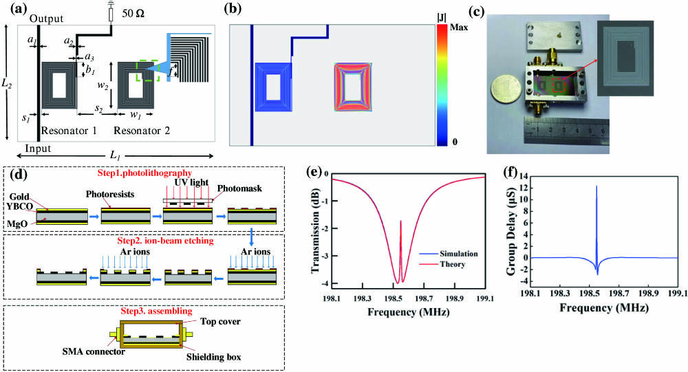
Figure 1.Design, fabrication, and simulation results. (a) Schematic diagram of the HTS coupled resonator circuit; (b) simulated current density of the HTS coupled resonators’ circuit at the transparent frequency; (c) photograph of the HTS coupled resonator circuit; (d) schematic diagram of fabrication process of the HTS circuit; (e) simulated and theoretical transmission spectra of the HTS coupled resonator circuit; (f) simulated group delay of the HTS coupled resonator circuit. The YBCO film has a conductivity of
The photograph of the fabricated sample is shown in Fig. 1(c). There are three steps to fabricate the proposed HTS device shown in Fig. 1(d). The circuit is fabricated on two separate MgO substrates with double-side coated YBCO HTS thin films. The electrical permittivity of MgO is more consistent throughout the whole layer than other substrates, such as
In the system depicted in Fig. 1(a), the output field is given as
In our experimental systems, the theoretically predicted parameters are shown as follows:
3. RESULTS AND DISCUSSION
Coupled-resonator-induced transparency can achieve EIT, Fano resonances, and ATS based on different central frequencies and coupling strength [43]. If there is a significant difference between
![]()
Figure 2.Simulation study of EIT, ATS, and Fano resonance of the coupled resonators. (a) Simulated results of transmission spectra as
As
Figure 3(a) shows the schematic diagram of the measurement setup. The circuit is measured with an Agilent N5230C vector network analyzer with an input power of 0 dBm at 65 K. The cryogenic condition is provided by a commercial Stirling cryocooler with an output power of 6 W. The fabricated device is fixed on the cold head of the cryocooler in a vacuum chamber. The circuit is tuned with sapphire tuning screws on the top cover to correct fabrication errors, and the center frequency of the high-Q resonator is altered to achieve an EIT response. Before measurement, the network analyzer is calibrated using an electronic calibrator to cancel out the loss and phase difference between reference line 1 and reference line 2, as shown in Fig. 3(a). After that, the transmission spectra, phase difference, and group delay, which is caused by the HTS device under test, are measured in a range of frequency. The simulated and measured results of transmission spectra and group delays are shown in Fig. 3(b) and Fig. 3(c), respectively. The measured results are in good agreement with the simulation results. The group delay is higher than 12.3 μs, which is much higher than the value previously reported. Moreover, the planar circuit is easy to be integrated, and the whole system, including the cryocooler, can be assembled as a portable device.
![]()
Figure 3.Experimental setup and results. (a) Schematic diagram of the measurement setup; (b) comparison between simulation and measurement results of the transmission spectra of the HTS coupled resonator circuit; (c) comparison between simulation and measurement results of the group delay of the HTS coupled resonator circuit; (d) measured results of transmission spectra as temperature varies; (e) measured group delay at the transparent frequency as temperature varies.
The conductivity of the HTS material strongly depends on the working temperature. The Q can be tuned by changing temperature, and the group delay of the circuit may be much larger. Figure 3(d) shows the temperature dependence of the transmission spectra. As the temperature decreases, the center frequency shifts slightly higher. The center frequency is 198.55 MHz at 65 K, and it shifts up to 198.64 MHz at 50 K while it shifts down to 198.38 MHz at 75 K. The group delay of the center frequency increases from 5.7 μs to 16.2 μs as the temperature decreases from 75 K to 50 K, as shown in Fig. 3(e). Lowering the temperature increases the group delay significantly, but a more severe working condition will be needed. In practical applications, the working temperature and performance of the device should be designed accordingly.
Table 1 shows some typical experimental systems implementing EIT in the microwave region. Some results only show the group delay, while the others only illustrate the group index. To compare the slow-wave properties clearly, we calculate the equivalent group index of our device with the following equation:
Comparison of the EIT-Induced Maximum Group Delay or Index in Different Physical Systems
| Experimental System | Frequency (GHz) | Group Delay (ns) | Group Index | Working Temperature (K) |
|---|---|---|---|---|
| Metal-based metamaterial [ | 3 | 10 | Room temperature | |
| Coupled metal resonators [ | 1.5 | 530 | Room temperature | |
| Metal-superconductor hybrid metamaterial [ | 10.5 | 300 | 3 | |
| Coupled superconducting coplanar waveguide cavity and nanomechanical oscillator [ | 6 | 0.2 | ||
| This work | 0.2 | 65 |
To just compare the order of magnitude as a conclusion, values in the table are approximated.
Here,
4. CONCLUSION
In conclusion, we propose and experimentally demonstrate an EIT response in a microwave circuit with coupled HTS resonators. We implement very large group delay at the VHF band, higher than 12.3 μs and 16.2 μs, with a working temperature of 65 K and 50 K, respectively. Simulated analysis of EIT, Fano resonances, and ATS shows EIT possesses the largest group delay, and this can be used for designing radio-frequency memory devices. Additionally, temperature-varying measurement shows the group delay increases significantly when the temperature is low. Our proposed method paves the way for studying EIT in the microwave region. Due to the high Q factor of the HTS resonator, the fabricated device shows great potential use for radio-frequency memory in the future.
References
[1] S. E. Harris, J. E. Field, A. Imamoğlu. Nonlinear optical processes using electromagnetically induced transparency. Phys. Rev. Lett., 64, 1107-1110(1990).
[2] K.-J. Boller, A. Imamoğlu, S. E. Harris. Observation of electromagnetically induced transparency. Phys. Rev. Lett., 66, 2593-2596(1991).
[3] A. M. Akulshin, S. Barreiro, A. Lezama. Electromagnetically induced absorption and transparency due to resonant two-field excitation of quasidegenerate levels in Rb vapor. Phys. Rev. A, 57, 2996-3002(1998).
[4] M. D. Eisaman, A. André, F. Massou, M. Fleischhauer, A. S. Zibrov, M. D. Lukin. Electromagnetically induced transparency with tunable single-photon pulses. Nature, 438, 837-841(2005).
[5] M. Mücke, E. Figueroa, J. Bochmann, C. Hahn, K. Murr, S. Ritter, C. J. Villas-Boas, G. Rempe. Electromagnetically induced transparency with single atoms in a cavity. Nature, 465, 755-758(2010).
[6] R. Röhlsberger, H.-C. Wille, K. Schlage, B. Sahoo. Electromagnetically induced transparency with resonant nuclei in a cavity. Nature, 482, 199-203(2012).
[7] L. V. Hau, S. E. Harris, Z. Dutton, C. H. Behroozi. Light speed reduction to 17 meters per second in ultracold atomic gases. Nature, 397, 594-598(1999).
[8] G. Morigi, J. Eschner, C. H. Keitel. Ground state laser cooling using electromagnetically induced transparency. Phys. Rev. Lett., 85, 4458-4461(2000).
[9] D. A. Braje, V. Balić, S. Goda, G. Y. Yin, S. E. Harris. Frequency mixing using electromagnetically induced transparency in cold atoms. Phys. Rev. Lett., 93, 183601(2004).
[10] N. Papasimakis, V. A. Fedotov, N. I. Zheludev, S. L. Prosvirnin. Metamaterial analog of electromagnetically induced transparency. Phys. Rev. Lett., 101, 253903(2008).
[11] P. Tassin, L. Zhang, T. Koschny, E. N. Economou, C. M. Soukoulis. Low-loss metamaterials based on classical electromagnetically induced transparency. Phys. Rev. Lett., 102, 053901(2009).
[12] L. Zhang, P. Tassin, T. Koschny, C. Kurter, S. M. Anlage, C. M. Soukoulis. Large group delay in a microwave metamaterial analog of electromagnetically induced transparency. Appl. Phys. Lett., 97, 241904(2010).
[13] J. Zhai, J. Zhou, L. Zhang, W. Hong. Behavioral modeling of power amplifiers with dynamic fuzzy neural networks. IEEE Microw. Wireless Compon. Lett., 20, 528-530(2010).
[14] J. Gu, R. Singh, X. Liu, X. Zhang, Y. Ma, S. Zhang, S. A. Maier, Z. Tian, A. K. Azad, H. T. Chen, A. J. Taylor, J. Han, W. Zhang. Active control of electromagnetically induced transparency analogue in terahertz metamaterials. Nat. Commun., 3, 1151(2012).
[15] P. Tassin, L. Zhang, R. Zhao, A. Jain, T. Koschny, C. M. Soukoulis. Electromagnetically induced transparency and absorption in metamaterials: the radiating two-oscillator model and its experimental confirmation. Phys. Rev. Lett., 109, 187401(2012).
[16] Z. Vafapour. Slow light modulator using semiconductor metamaterial. Proc. SPIE, 10535, 105352A(2018).
[17] R. Yang, Q. Fu, Y. Fan, W. Cai, K. Qiu, W. Zhang, F. Zhang. Active control of EIT-like response in a symmetry-broken metasurface with orthogonal electric dipolar resonators. Photon. Res., 7, 955-960(2019).
[18] Q. Xu, S. Sandhu, M. L. Povinelli, J. Shakya, S. Fan, M. Lipson. Experimental realization of an on-chip all-optical analogue to electromagnetically induced transparency. Phys. Rev. Lett., 96, 123901(2006).
[19] Q. Xu, P. Dong, M. Lipson. Breaking the delay-bandwidth limit in a photonic structure. Nat. Phys., 3, 406-410(2007).
[20] M. F. Limonov, M. V. Rybin, A. N. Poddubny, Y. S. Kivshar. Fano resonances in photonics. Nat. Photonics, 11, 543-554(2017).
[21] N. Liu, L. Langguth, T. Weiss, J. Kästel, M. Fleischhauer, T. Pfau, H. Giessen. Plasmonic analogue of electromagnetically induced transparency at the Drude damping limit. Nat. Mater., 8, 758-762(2009).
[22] R. Taubert, M. Hentschel, J. Kästel, H. Giessen. Classical analog of electromagnetically induced absorption in plasmonics. Nano Lett., 12, 1367-1371(2012).
[23] G. C. Dyer, G. R. Aizin, S. J. Allen, A. D. Grine, D. Bethke, J. L. Reno, E. A. Shaner. Induced transparency by coupling of Tamm and defect states in tunable terahertz plasmonic crystals. Nat. Photonics, 7, 925-930(2013).
[24] C. W. Hsu, B. G. DeLacy, S. G. Johnson, J. D. Joannopoulos, M. Soljačić. Theoretical criteria for scattering dark states in nanostructured particles. Nano Lett., 14, 2783-2788(2014).
[25] A. A. Abdumalikov, O. Astafiev, A. M. Zagoskin, Y. A. Pashkin, Y. Nakamura, J. S. Tsai. Electromagnetically induced transparency on a single artificial atom. Phys. Rev. Lett., 104, 193601(2010).
[26] P. M. Anisimov, J. P. Dowling, B. C. Sanders. Objectively discerning Autler-Townes splitting from electromagnetically induced transparency. Phys. Rev. Lett., 107, 163604(2011).
[27] J. Wu, B. Jin, J. Wan, L. Liang, Y. Zhang, T. Jia, C. Cao, L. Kang, W. Xu, J. Chen, P. Wu. Superconducting terahertz metamaterials mimicking electromagnetically induced transparency. Appl. Phys. Lett., 99, 161113(2011).
[28] C. Kurter, P. Tassin, L. Zhang, T. Koschny, A. P. Zhuravel, A. V. Ustinov, S. M. Anlage, C. M. Soukoulis. Classical analogue of electromagnetically induced transparency with a metal-superconductor hybrid metamaterial. Phys. Rev. Lett., 107, 043901(2011).
[29] X. Zhou, F. Hocke, A. Schliesser, A. Marx, H. Huebl, R. Gross, T. J. Kippenberg. Slowing, advancing and switching of microwave signals using circuit nanoelectromechanics. Nat. Phys., 9, 179-184(2013).
[30] O. Limaj, F. Giorgianni, A. Di Gaspare, V. Giliberti, G. De Marzi, P. Roy, M. Ortolani, X. Xi, D. Cunnane, S. Lupi. Superconductivity-induced transparency in terahertz metamaterials. ACS Photon., 1, 570-575(2014).
[31] C. Zhang, J. Wu, B. Jin, X. Jia, L. Kang, W. Xu, H. Wang, J. Chen, M. Tonouchi, P. Wu. Tunable electromagnetically induced transparency from a superconducting terahertz metamaterial. Appl. Phys. Lett., 110, 241105(2017).
[32] J. Joo, J. Bourassa, A. Blais, B. C. Sanders. Electromagnetically induced transparency with amplification in superconducting circuits. Phys. Rev. Lett., 105, 073601(2010).
[33] Z. Vafapour, M. Dutta, M. A. Stroscio. Sensing, switching and modulating applications of a superconducting THz metamaterial. IEEE Sens. J., 21, 15187-15195(2021).
[34] A. H. Safavi-Naeini, T. P. M. Alegre, J. Chan, M. Eichenfield, M. Winger, Q. Lin, J. T. Hill, D. E. Chang, O. Painter. Electromagnetically induced transparency and slow light with optomechanics. Nature, 472, 69-73(2011).
[35] H. Xiong, Y. Wu. Fundamentals and applications of optomechanically induced transparency. Appl. Phys. Rev., 5, 031305(2018).
[36] D. U. Smith, H. Chang, K. A. Fuller, A. T. Rosenberger, R. W. Boyd. Coupled-resonator-induced transparency. Phys. Rev. A, 69, 063804(2004).
[37] K. Totsuka, N. Kobayashi, M. Tomita. Slow light in coupled-resonator-induced transparency. Phys. Rev. Lett., 98, 213904(2007).
[38] F.-C. Lei, M. Gao, C. Du, Q.-L. Jing, G.-L. Long. Three-pathway electromagnetically induced transparency in coupled-cavity optomechanical system. Opt. Express, 23, 11508-11517(2015).
[39] C. Wang, X. Jiang, G. Zhao, M. Zhang, C. W. Hsu, B. Peng, A. D. Stone, L. Jiang, L. Yang. Electromagnetically induced transparency at a chiral exceptional point. Nat. Phys., 16, 334-340(2020).
[40] B. Wu, J. F. Hulbert, E. J. Lunt, K. Hurd, A. R. Hawkins, H. Schmidt. Slow light on a chip via atomic quantum state control. Nat. Photonics, 4, 776-779(2010).
[41] S. D. Berger. The spectrum of a digital radio frequency memory linear range gate stealer electronic attack signal. Proceedings of the 2001 IEEE Radar Conference, 27-30(2001).
[42] M. Amin, R. Ramzan, O. Siddiqui. Slow wave applications of electromagnetically induced transparency in microstrip resonator. Sci. Rep., 8, 2357(2018).
[43] B. Peng, Ş. K. Özdemir, W. Chen, F. Nori, L. Yang. What is and what is not electromagnetically induced transparency in whispering-gallery microcavities. Nat. Commun., 5, 5082(2014).


Set citation alerts for the article
Please enter your email address

© Copyright 2018-2021 | Chinese Laser Press. All Rights Reserved 沪ICP备15018463号-20