
Zhiqiang Liu, Yiyao Hu, Mao Ye. Liquid Crystal Axicon[J]. Acta Optica Sinica, 2022, 42(8): 0823001
- Acta Optica Sinica
- Vol. 42, Issue 8, 0823001 (2022)
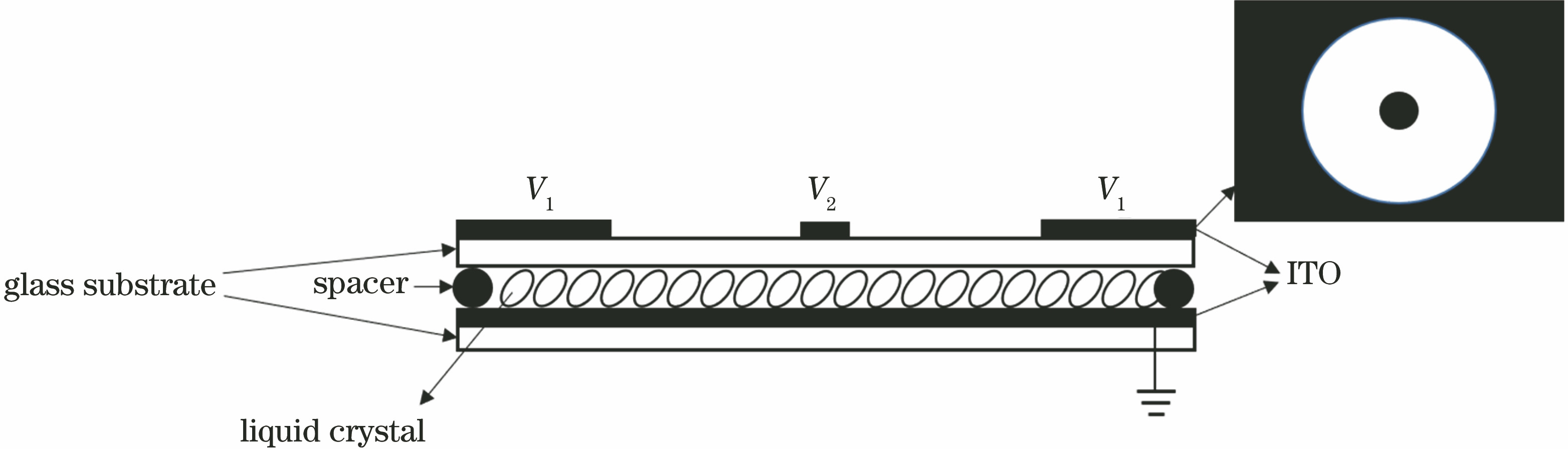
Fig. 1. Liquid crystal axicon structure
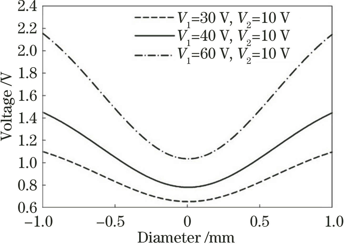
Fig. 2. Simulation results of electric field of liquid crystal axicon
Fig. 3. Response curve of liquid crystal to electric field
Fig. 4. Wavefront interferograms of liquid crystal axicon. (a) V1=30 V, V2=10 V; (b) V1=40 V, V2=10 V; (c) V1=60 V, V2=10 V
Fig. 5. Wavefront fitting diagram of lens under different voltages
Fig. 6. Schematic diagram of generating local hollow beam
Fig. 7. Focus images of laser by system. (a) V1=30 V, V2=10 V; (b) V1=40 V, V2=10 V; (c) V1=60 V, V2=10 V
Fig. 8. Experimental device for imaging with extended depth of field realized by using liquid crystal axicon
Fig. 9. Effect of extended depth of field imaging
Fig. 10. System imaging effects with and without voltage applied to liquid crystal axicon. (a) Imaging effects when liquid crystal axicon is not working; (b) imaging effects when liquid crystal axicon is working
Fig. 11. Change of MTF30 with object distance
|
Table 1. Calculation results of cone angle of liquid crystal axicon

Set citation alerts for the article
Please enter your email address
© Copyright 2018-2021 | Chinese Laser Press. All Rights Reserved 沪ICP备15018463号-20