
Yufei Jia, Yufei Wang, Xuyan Zhou, Linhai Xu, Pijie Ma, Jingxuan Chen, Hongwei Qu, Wanhua Zheng, "Narrow vertical beam divergence angle for display applications of 645 nm lasers," Chin. Opt. Lett. 19, 101401 (2021)
- Chinese Optics Letters
- Vol. 19, Issue 10, 101401 (2021)
Abstract
1. Introduction
Applications of laser diodes (LDs) have been widely spreading into many areas, from the industrial manufacturing like welding and cutting to daily life such as data storage and telecommunication. Red-emitting laser sources play an important role in the medical field and digital appliances[
In this Letter, we adopt the structure of the mode expansion layer to narrow down the vertical beam divergence and analyze the mode behavior in the vertical direction. A low vertical divergence angle of 10.94° is realized in the experiment. The peak power of the broad area (BA) laser can reach 0.94 W, limited by the thermal rollover under continuous-wave (CW) operation. Furthermore, we fabricate the low coherence red LD device, which can achieve speckle contrast of 3.6% and peak power of 1.42 W under pulsed operation. This red LD can also realize the directional emission in both lateral and vertical directions.
2. Passive Mode Analysis and Structure Design
The refractive index of AlGaInP is critical to the calculation of the near-field amplitude, which further influences the far-field intensity profile. We adopt the modified single effective oscillator (MSEO) and related parameters to ensure the accuracy of refractive index of the layers[
Sign up for Chinese Optics Letters TOC. Get the latest issue of Chinese Optics Letters delivered right to you!Sign up now
![]()
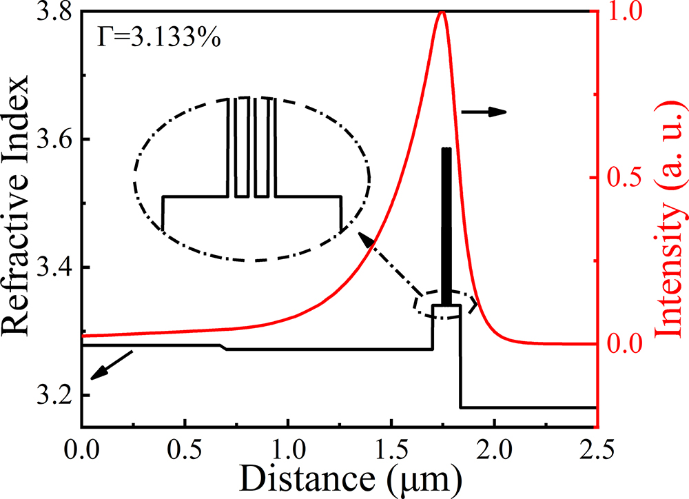
Figure 1.Schematic of the sectional refractive index distribution (left axis) and the optical NFP distribution (right axis). The inset shows the detail of the active region.
In the epitaxial direction, the following layers include 0.1 µm GaInP:Si
The maximum conduction band offset (
![]()
Figure 2.Calculated conduction energy band diagram at different doping levels. The inset shows the ΔEc between the waveguide layer and the p-cladding layer at different doping levels.
The thicknesses of the cladding layer (
![]()
Figure 3.(a) Dependence of calculated Γ, vertical divergence, and RF/H on dME; (b) dependence of vertical divergence on dn−cladding.
![]()
Figure 4.Simulated far-field pattern (FFP) in the fast axis.
In order to realize the low coherence, we prefer to have a number of modes lasing simultaneously by designing the cavity structure. We directly fabricate the low coherence LD according to the good results in our previous work[
3. Device Fabrication and Results
The epitaxial layer is grown by metal organic chemical vapor deposition (MOCVD) on a Si-doped misoriented GaAs substrate tilted 15° off (100) toward [111]. The BA lasers are formed by photolithography and dry etching, and
Uncoated BA lasers are fabricated to obtain parameters such as the internal quantum efficiency (
![]()
Figure 5.(a) Cavity length dependence of the inverse external differential quantum efficiency; (b) threshold current density versus the inverse cavity length.
We adopt
![]()
Figure 6.Experimental L–I–V and WPE characteristics for 100 µm BA laser with a 1500 µm long cavity. The laser device is operated with coated AR of 10% and HR of 99% under 3 A CW at 20°C heatsink temperature. The inset shows the spectrum at 1.5 A CW.
The contrast of the vertical far-field profile is presented in Fig. 7. We obtain the vertical far-field divergence as low as 10.94° (FWHM) and 19.7° (
![]()
Figure 7.FFP of simulation and experiment. The dashed line indicates
To the best of our knowledge, the vertical divergence of 10.94° is the smallest for the red LD based on the mode expansion layer, other than the longitudinal photonic crystal structure.
Figure 8(a) shows the schematic of the low coherence red LD structure. The sizes of the R,
![]()
Figure 8.(a) Schematic of the low coherence red LD structure; (b) L–I–V curves; (c) the spectrum at 10 A; (d) the FFP at 10 A.
The vertical divergence angles between the low coherence LD and BA LD are different. We doubt that the possible reasons are the lateral mode oscillation and the different test conditions due to the test equipment.
We characterize the low coherence by the speckle contrast. Figure 9(a) shows the schematic of the experimental setup of the speckle measurement. The light emitted from laser is coupled into a fiber (
![]()
Figure 9.(a) Schematic of the experimental setup of the speckle measurement; (b) speckle pattern of low coherence red LD structure; (c) speckle pattern of BA laser.
4. Conclusion
We have demonstrated red LDs with a narrow vertical far field in the 645 nm range. An efficient mode expansion layer is designed to produce a strong penetration of the near-field distribution, which is beneficial to narrow down the FFP. A narrow vertical far-field angle of 10.94° is achieved experimentally. The maximum output power of 0.94 W at 2.7 A, limited by the thermal rollover, is achieved under the CW condition.
We have realized red LDs with a low coherence and directional emission with this epitaxy structure. The peak power of 1.42 W and the lateral divergence of 8.3° are achieved under pulsed operation. The speckle contrast is reduced to 3.6%, which means it has a bright prospect in laser display. With the optimization of epitaxial layers, the low coherence red LD can operate at the CW condition.
References
[1] M. M. He, S. Chen, Q. X. Na, S. J. Luo, H. Y. Zhu, Y. Li, C. W. Xu, D. Y. Fan. Watt-level Pr3+:YLF deep red laser pumped by a fiber-coupled blue LD module or a single-emitter blue LD. Chin. Opt. Lett., 18, 011405(2020).
[2] T. Yagi, H. Nishiguchi, Y. Yoshida, M. Miyashita, M. Sasaki, Y. Sakamoto, K. Ono, Y. Mitsui. High-power high-efficiency 660-nm laser diodes for DVD-R/RW. IEEE J. Sel. Top. Quantum Electron., 9, 1260(2003).
[3] C. Y. Chen, H. T. Chang, T. J. Chang, C. H. Chuang. Full-color and less-speckled modified Gerchberg–Saxton algorithm computer-generated hologram floating in a dual-parabolic projection system. Chin. Opt. Lett., 13, 110901(2015).
[4] H. Kawanishi. IR/R/G/B laser diodes for multi-wavelength applications. Opt. Rev., 26, 152(2019).
[5] Z. Y. Xu. Laser displays—new display technology for next generation. Laser Infrared, 36, 737(2006).
[6] T. Nishida, K. Kuramoto, Y. Iwai, T. Fujita, T. Yagi. Multiemitter 638-nm high-power broad area laser diodes for display application. Opt. Eng., 58, 086113(2019).
[7] M. Hagimoto, S. Miyamoto, Y. Kimura, H. Fukai, M. Hashizume, S. Kawanaka. USHIO 3.5W red laser diode for projector light source. Proc. SPIE, 10939, 109391I(2019).
[8] K. Paschkel, G. Blume, D. Feise, J. Pohl, B. Sumpf. Watt-level red-emitting diode lasers and modules for display applications. Opt. Rev., 23, 146(2016).
[9] B. Sverdlov, H.-U. Pfeiffer, E. Zibik, S. Mohrdiek, T. Pliska, M. Agresti, N. Lichtenstein. Optimization of fiber coupling in ultra-high power pump modules at λ = 980 nm. Proc. SPIE, 8605, 860508(2013).
[10] P. Unger, G.-L. Bona, R. Germann, P. Roentgen, D. J. Webb. Low-threshold strained GaInP quantum-well ridge lasers with AlGaAs cladding layers. IEEE J. Quantum Electron., 29, 1880(1993).
[11] K. Hamada, M. Wada, H. Shimizu, M. Kume, F. Susa, T. Shibutani, N. Yoshikawa, K. Itoh, G. Kano, I. Teramoto. A 0.2 W CW laser with buried twin-ridge substrate structure. IEEE J. Quantum Electron., 21, 623(1985).
[12] N. B. Zvonkov, B. N. Zvonkov, A. V. Ershov, E. A. Uskova, G. A. Maksimov. Semiconductor lasers emitting at the 0.98 µm wavelength with radiation coupling-out through the substrate. Quantum Electron., 28, 605(1998).
[13] V. Shchukin, N. Ledentsov, K. Posilovic, V. Kalosha, T. Kettler, D. Seidlitz, M. Winterfeldt, D. Bimberg, N. Y. Gordeev, L. Y. Karachinsky, I. I. Novikov, Y. M. Shernyakov, A. V. Chunareva, M. V. Maximov, F. Bugge, M. Weyers. Tilted wave lasers: a way to high brightness sources of light. IEEE J. Quantum Electron., 47, 1014(2011).
[14] S. Zhao, A. Qi, M. Wang, H. Qu, Y. Lin, F. Dong, W. Zheng. High-power high-brightness 980 nm lasers with >50% wall-plug efficiency based on asymmetric super large optical cavity. Opt. Express, 26, 3518(2018).
[15] L. Liu, H. Qu, Y. Liu, Y. Wang, A. Qi, X. Guo, P. Zhao, Y. Zhang, W. Zheng. Design and analysis of laser diodes based on the longitudinal photonic band crystal concept for high power and narrow vertical divergence. IEEE J. Sel. Top. Quantum Electron, 21, 1900107(2015).
[16] P. M. Smowton, G. M. Lewis, M. Yin, H. D. Summers, G. Berry, C. C. Button. 650-nm lasers with narrow far-field divergence with integrated optical mode expansion layers. IEEE J. Sel. Top. Quantum Electron, 5, 735(1999).
[17] B. Qiu, O. P. Kowalski, S. McDougall, B. Schmidt, J. H. Marsh. High-performance red lasers with low beam divergence. IEEE Photon. J., 1, 172(2009).
[18] P. M. Smowton, S. N. Elliott. Manufacturing-tolerant compact red-emitting laser diode designs for next generation applications. IET Optoelectron., 9, 75(2015).
[19] B. Redding, A. Cerjan, X. Huang, M. L. Lee, A. D. Stone, M. A. Choma, H. Cao. Low spatial coherence electrically pumped semiconductor laser for speckle-free full-field imaging. Proc. Natl. Acad. Sci. USA, 112, 1304(2015).
[20] K. Kim, S. Bittner, Y. Zeng, SF. Liew, Q. Wang, H. Cao. Electrically pumped semiconductor laser with low spatial coherence and directional emission. Appl. Phys. Lett., 115, 071101(2019).
[21] Y. Jia, Y. Wang, L. Xu, S. Zhao, A. Qi, W. Zheng. Low-spatial coherence electrically pumped red-emitting semiconductor laser. Proc. SPIE, 10812, 108120V(2018).
[22] L. Xu, Y. Wang, Y. Jia, W. Zheng. Low-coherence, high-power, high-directional electrically driven dumbbell-shaped cavity semiconductor laser at 635 nm. Opt. Lett., 45, 5097(2020).
[23] M. A. Afromowitz. Refractive index of Ga1−xAlxAs. Solid State Commun., 15, 59(1974).
[24] G. Hatakoshi, K. Itaya, M. Ishikawa, M. Okajima, Y. Uematsu. Short-wavelength InGaAlP visible laser diodes. IEEE J. Quantum Electron., 27, 1476(1991).
[25] D. P. Bour. Strained GaxIn1-xP-(AlGa)0.5In0.5P heterostructures and quantum-well laser diodes. IEEE J. Quantum Electron., 30, 593(1994).


Set citation alerts for the article
Please enter your email address

© Copyright 2018-2021 | Chinese Laser Press. All Rights Reserved 沪ICP备15018463号-20