• Journal of Infrared and Millimeter Waves
  • Vol. 41, Issue 4, 785 (2022)
Shan-Zhe YU1, Ya-Cong ZHANG1、*, Yu-Ze NIU1, Ye ZHOU1, Yi ZHUO1, Ding MA2, Wen-Gao LU1、**, Zhong-Jian CHEN1, and Xiang-Yang LI2
Author Affiliations
  • 1National Key Laboratory of Science and Technology on Micro/Nano Fabrication,School of Integrated Circuits,Peking University,Beijing 100871,China
  • 2Key Laboratory of Infrared Imaging Materials and Detectors,Shanghai Institute of Technical Physics,Chinese Academy of Sciences,Shanghai 200083,China
  • show less
    DOI: 10.11972/j.issn.1001-9014.2022.04.019 Cite this Article
    Shan-Zhe YU, Ya-Cong ZHANG, Yu-Ze NIU, Ye ZHOU, Yi ZHUO, Ding MA, Wen-Gao LU, Zhong-Jian CHEN, Xiang-Yang LI. A 48 mW DROIC with 15-bit pixel-level ADC for 640×512 mid-wave infrared imagers[J]. Journal of Infrared and Millimeter Waves, 2022, 41(4): 785 Copy Citation Text show less
    Conventional digital pixel with SS-ADC
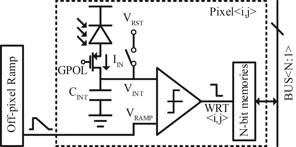
    Fig. 1. Conventional digital pixel with SS-ADC
    Block diagram of the proposed DROIC with the novel pixel-level SS-ADC
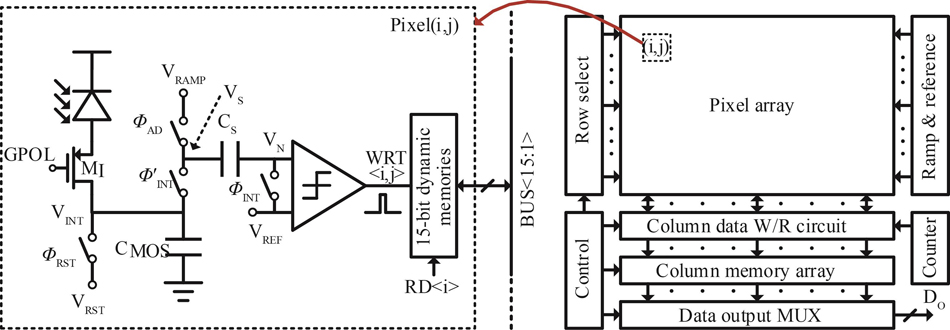
    Fig. 2. Block diagram of the proposed DROIC with the novel pixel-level SS-ADC
    Timing diagram of the proposed DROIC
    Fig. 3. Timing diagram of the proposed DROIC
    (a)The circuit diagram,and(b)the timing diagram of proposed power-self-adaptive pulse comparator:(a)(b)
    Fig. 4. (a)The circuit diagram,and(b)the timing diagram of proposed power-self-adaptive pulse comparator:(a)(b)
    Simulation results of IC when VINT equals (a) 0.8V, (b) 1.5 V, respectively
    Fig. 5. Simulation results of IC when VINT equals (a) 0.8V, (b) 1.5 V, respectively
    The circuit diagram of the pixel dynamic memory and the column data W/R circuit
    Fig. 6. The circuit diagram of the pixel dynamic memory and the column data W/R circuit
    (a)The microphotograph of the DROIC,(b)custom-designed PCB to test the DROIC
    Fig. 7. (a)The microphotograph of the DROIC,(b)custom-designed PCB to test the DROIC
    the layout of 2×2 pixels
    Fig. 8. the layout of 2×2 pixels
    Measured VRAMP captured by oscilloscope
    Fig. 9. Measured VRAMP captured by oscilloscope
    SNR histogram of the whole pixel array at the full well
    Fig. 10. SNR histogram of the whole pixel array at the full well
    When VRST=1.35 V(a)the gray-scale image of the DROIC,(b)the gray-scale image of FPN
    Fig. 11. When VRST=1.35 V(a)the gray-scale image of the DROIC,(b)the gray-scale image of FPN
    The digital output versus the reset voltage VRST
    Fig. 12. The digital output versus the reset voltage VRST
    The non-linearity versus the reset voltage VRST
    Fig. 13. The non-linearity versus the reset voltage VRST
    Parameter51211This work
    Technology process /nm180-90180
    Pixel array640×5121 024x76832×32640×512
    Pixel size /μm10101515
    Frame rate /Hz180100400120
    ADC resolution /bit13141515
    Power consumption /mW1101001.448
    Charge capacity /e-2M2.6M2.4M8.8M
    Noise voltage */μV/ Peak SNR */dB160/N.A.N.A./83**N.A./79116/84
    FoM**/(pJ/pixelstep)22877.610437.3
    Table 1. Performance comparison of DROICs
    Shan-Zhe YU, Ya-Cong ZHANG, Yu-Ze NIU, Ye ZHOU, Yi ZHUO, Ding MA, Wen-Gao LU, Zhong-Jian CHEN, Xiang-Yang LI. A 48 mW DROIC with 15-bit pixel-level ADC for 640×512 mid-wave infrared imagers[J]. Journal of Infrared and Millimeter Waves, 2022, 41(4): 785
    Download Citation