A sub-harmonic monolithic mixer with a center frequency of 0.825 THz is developed based on GaAs monolithic microwave integrated circuit technology. The parasitic parameters of the anti-parallel Schottky diode at the terahertz frequency are analyzed to improve the circuit design. The monolithic circuit is suitable for terahertz devices with the characteristics of high integration and little fabrication deviation. Meanwhile, the beamlead circuit is used to reduce the loss of substrate and installation position offset. Measured results show that the single-sideband (SSB) conversion loss of the mixer is lower than 33 dB in the frequency range 0.81~0.84 THz, and the minimum SSB conversion loss is 28 dB.
The terahertz wave is between microwave and optical wave,which has huge applications[1]. Terahertz waves have a low quantum energy,good security,and wide frequency band,which is worthy of academic research and applications[2–4]. These waves have wide application prospects in the fields of security imaging,terahertz communication,and terahertz spectrum analysis[5-6]. Research on devices and systems at high terahertz frequencies is sparse due to the limitation of monolithic microwave integrated circuit technology and the lack of terahertz sources. The development of terahertz devices provides the technical basis for detecting ice-cloud information,which can be further improved through detection above 0.8 THz,at which meteorological changes can be more accurately forecast and some natural disasters prevented in advance[7]. With increasingly deeper exploration of terahertz applied fields,terahertz devices are being developed with higher frequency and better performance[8–14]. Thomas designed an 835∼900 GHz fundamental balanced mixer with 9.25 dB conversion loss[15]. And Thomas,et al. designed an 874 GHz sub-harmonic balanced mixer. The optimal conversion loss of this mixer is 10 dB and the 3 dB bandwidth ranges from 820 to 920 GHz[16]. Zhang Bo,et al. designed a 1.1 THz tenth-harmonic mixer based on a planar GaAs Schottky diode. Measurement results show that the conversion loss is less than 55 dB in the frequency range 1.03∼1.154 THz[17].
The design of a sub-harmonic mixer above 0.8 THz and the associated processing measurements have been completed in the present work. The core component of the proposed terahertz mixer is an anti-parallel Schottky diode,which shows a complex high frequency parasitic effect in the terahertz range. The analysis and modeling of Schottky diodes is the key to the design of a monolithic circuit,which will bring more advantages to realize matching circuit and to achieve better performance of mixer [18-19]. Further study on the high frequency parasitic parameter model of a Schottky diode is of great value for the design of a 0.825 THz monolithic mixer circuit.
1 Schottky diode modeling
A Schottky diode is an important component of conversion devices in terahertz. It is necessary to analyze the diode model deeply for a better circuit match to improve device performance. The structure of a Schottky diode consists of a high electron mobility substrate,low doping buffer layer,high doping epitaxial layer,and upper metal structure,as shown in Fig. 1.
Figure 1.Three-dimensional cross-sectional view of Schottky diode
A Schottky diode is mainly composed of intrinsic parameters and high frequency parasitic parameters. The intrinsic parameters reflect the DC characteristics of Schottky diodes,including ideal factor ,saturation current ,zero-bias junction capacitance ,and series resistance [20]. These characteristics determine the cutoff frequency of the diode and play an important role in the matching of the entire circuit.
,,,,.
In this design,the Schottky diode anode diameter is 0.8 µm and epitaxial layer thickness 0.1 µm. According to the above formula,,,and .
However,the high frequency parasitic parameters of the diode cannot be ignored because of the great influence on the design of devices in terahertz. The high frequency effect of a Schottky diode is seldom studied due to the vacancy of on-chip test probe platforms. A detailed theoretical analysis and simulation verification of high-frequency parasitic parameter extraction are carried out by the parameter matrix,which mainly includes the parasitic capacitance between anode and cathode pads,parasitic inductance and parasitic resistance of the air bridge finger,and parasitic capacitance between air bridge and pad[21–24]. The top view of the anti-parallel Schottky diode is shown in Fig. 2.
The anode and cathode pad structure can be equivalent to the π-type circuit composed of capacitance and inductance ,the finger can be equivalent to the series circuit of finger inductance and finger resistance ,and the anode column part can be equivalent to the parallel circuit of parasitic capacitance between finger and pad parallel capacitance and resistance of the Schottky-junction contact. The equivalent circuit of an anti-parallel Schottky diode for four-step parameter extraction is shown in Fig. 3,where ① is the equivalent circuit of the pad,② is the equivalent circuit between the anode and cathode pad,③ is the equivalent circuit of the finger,and ④ is the equivalent circuit between the finger and pad.
Figure 3.Equivalent circuit of anti-parallel Schottky diode
The Y parameters of the anode or cathode pad structure ,no finger structure ,finger connected structure ,and finger pad part ,are calculated as follows,where is the number of fingers,.
.
The Y parameters of each part can be calculated from the simulation,where is the no finger structure parameter; the finger short structure parameter,where and the no Schottky-junction structure parameter.
.
From the above simulated Y-parameters,the component values of the parasitic equivalent circuit are the following:
,,,, .
According to the above formula and the simulated S parameters of the Schottky diode,the high frequency parasitic parameters can be calculated as follows:,where varies with the distance between the anode and cathode pad. ,,and ,which are related to finger width and distance between fingers.
,
is the mutual inductance between two fingers,which is a special parasitic parameter of an anti-parallel Schottky diode. The anode pad,cathode pad,and fingers play an important role in the formation of high frequency parasitic parameters. A more reasonable design of a Schottky diode model can reduce high-frequency parasitic parameters to achieve a better design.
2 Mixer design
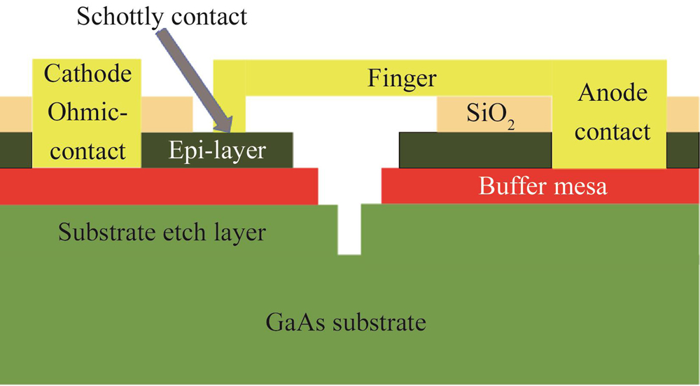
A beamlead monolithic circuit is used to realize the installation of the circuit and cavity in the design of the 0.825 THz sub-harmonic mixer,which not only reduces the loss caused by the dielectric substrate,but also reduces the installation position offset. The design of the sub-harmonic mixer mainly includes radio frequency (RF)and local oscillator (LO)probes,LO and intermediate frequency (IF)low-pass filters,and the anti-parallel Schottky diode. A WR1 rectangular waveguide is used as the RF waveguide in the frequency range 0.75∼1.1 THz,and a WR2.2 rectangular waveguide as the LO waveguide in the frequency range 0.33∼0.5 THz. The beam lead circuit is installed in the cavity with a small amount of conductive adhesive [25]. The proposed 0.825 THz mixer architecture and assembled mixer block are shown in Fig. 4.
Figure 4.Proposed 0.825 THz mixer architecture and assembled mixer block
Simulated results show that the SSB conversion loss of this mixer is 9 dB in the range 0.815∼0.835 THz,and the minimum SSB conversion loss is 7.8 dB. The simulated conversion loss of the 0.825 THz sub-harmonic mixer is shown in Fig. 5.
For the proposed 0.825 THz mixer design,the LO low-pass filter (LPF)adopts the form of three high and low impedance lines,which has a simple structure and wide bandwidth. The IF LPF [26] is different from the LO LPF and has compact microstrip resonating cell (CMRC)structure. The length of the LO LPF is 149 µm and the length of the CMRC for the IF LPF is 230 µm. Simulated results from the two LPFs are shown in Fig. 6.
The performance of the proposed 0.825 THz subharmonic mixer was measured by fixed IF frequency,and the construction of the subharmonic mixer test platform is depicted in Fig. 7. The RF and LO are input into the mixer,and the IF power is measured by a spectrometer.
Figure 7.Sub-harmonic mixer performance measurement platform for 0.825 THz
The signal generator operates at 11.1∼11.7 GHz. To provide the 0.4∼0.42 THz LO signal with 4 mW,the signal generator was cascaded by a sextupler,attenuator,doubler and tripler. The RF source is provided by a 0.75∼1.1 THz extender,and the IF output is obtained by a spectrum analyzer. The measured performance of the proposed 0.825 THz sub-harmonic mixer is shown in Fig. 8. It can be observed from the figure that the measured SSB conversion loss is 28∼33 dB over the frequency range 0.81∼0.84 THz,and the minimum SSB conversion loss is 28 dB at 0.836 THz.
There is difference between the measured and simulated results due to the circuit size sensitivity of terahertz devices,for which a small deviation will have a great impact on the final results. Because the ratio between circuit size and wavelength cannot be ignored,the processes of monolithic circuit processing,cavity processing,and installation have great influence. During measurement,the loss of the RF source is caused by the gap between the flange of the extender and that of the RF waveguide,the position deviation of the waveguide port,and the roughness of waveguide. There is approximately a 5 dB loss when the gap between the two flanges is 30 µm,and approximately a 3 dB loss when the position deviation of the waveguide port is 40 µm in simulation. It is easy to produce position deviation in the connection of measurement equipment,which cannot be ignored at terahertz frequencies. More attention will be paid to the avoidance of assembly deviation in the next planned design. The deviation between the simulated and measured results may be due to the inaccurate simulation model,processing error,assembly error and measurement error. Although many uncontrollable deviations have an influence on the performance of the proposed 0.825 THz mixer,its design is preliminarily realized.
4 Conclusions
A monolithic mixer is designed in the form of a beamlead circuit based on a 15 µm thick GaAs substrate. A more reasonable anti-parallel Schottky diode model is designed based on the analysis of the intrinsic parameters and high-frequency parasitic effect of the Schottky diode. Measured results show that the SSB conversion loss of the proposed 0.825 THz mixer is lower than 33 dB in the range 0.81∼0.84 THz,and the minimum SSB conversion loss is 28 dB at 0.836 THz. The deviation that may be introduced in the measurement of a terahertz monolithic mixer can influence the conversion loss of the mixer. The measured results of the 0.825 THz monolithic mixer prove that monolithic circuit design will become one of the important directions of future terahertz device design. More in-depth analysis of the diode model,greater tolerance in circuit design,and smaller deviation in the assembly measurement process are several problems that will be solved in the monolithic design.
[9] Ge LIU, Bo ZHANG, Li-Sen ZHANG et al. 0.42 THz subharmonic mixer based on 3D precisely modeled diode. Journal of infrared and millimeter waves, 37, 338-343(2018).
[11] Jun JIANG, Yue HE, Cheng WANG et al. 0.67 THz sub-harmonic mixer based on Schottky diode and hammer-head filter. Journal of Infrared Millimeter Waves, 35, 418-424(2016).
[13] Yan-Fei MAO, E Shi-Ju, Klaus SCHMALZ, Klaus SCHMALZ等. 一种低功耗245 GHz次谐波接收机. 红外与毫米波学报, 38, 739-744(2019).
et alA low power 245 GHz subharmonic receiver. Journal of Infrared Millimeter Waves, 38, 739-744(2019).
[14] Ge LIU, Bo ZHANG, Li-Sen ZHANG et al. 330 GHz GaAs monolithic integrated sub-harmonic mixer. Journal of infrared and millimeter waves, 36, 252-256(2017).