Jun-Jun QI, Hong-Liang LYU, Lin CHENG, Yu-Ming ZHANG, Yi-Men ZHANG, Feng-Guo ZHAO, Lan-Yan DUAN. A distributed small signal equivalent circuit modeling method for InP HEMT[J]. Journal of Infrared and Millimeter Waves, 2022, 41(2): 511
Copy Citation Text
A distributed small signal equivalent circuit modeling method for InP high electron mobility transistor (HEMT) was presented. The distributed capacitance effect was considered in the adopted model, which is characterized by adding three distributed capacitances. For accurate modeling, the parasitic inductances are extracted first,considerig the errors introduced by the parasitic inductances when extracting the parasitic capacitance first. The validity of the proposed small signal modeling method has been verified with excellent agreement between the measured and modeled results up to 50 GHz for InP HEMT. In addition, the S-parameters’ modeling error is less than 4% in 2 ~ 50 GHz, which also proves the high accuracy of the proposed modeling method.
With the continuous development of RF wireless communication system,the demand for high-performance and low-cost RF solutions is increasing [1]. Compare to traditional Si and Ge-based CMOS devices,InP HEMT transistors have better frequency response characteristics,power density and breakdown voltage,which makes InP HEMT transistors become an excellent candidate for many monolithic microwave integrated circuits(MMICs)working at GHz frequency range [2]. As an important link between transistors and circuits,a large signal model which can accurately simulate dc,S-parameters and large signal characteristics determines the accuracy of circuits. Meanwhile,small signal model is the approximation of the large signal model at a single bias point [3]. Therefore,the accuracy of the large signal model depends mostly on the small signal equivalent circuit model which can reflect the physical and electrical properties of the device [4].
In the past decades,various extraction techniques,including numerical optimization method [5] and direct extraction method [6-7]have been developed. The numerical optimization method uses the numerical method to find the optimal parameter value. Although it is very accurate,it depends largely on the initial value of the parameter and may not converge. The direct extraction method uses the analytical equations to obtain the expression of each parameter without optimization,but it is difficult to be applied to small signal model with complex topology.
In order to solve these problems,the method combining numerical optimization and direct extraction method is used to extract the equivalent circuit parameters. This method takes the parameter value obtained by the direct extraction method as the initial value of the optimization method,which not only maintains the accuracy of the optimization method,but also avoids the convergence problem.
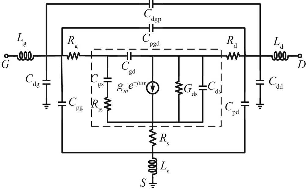
1 A distributed small signal equivalent circuit model
A distributed small signal equivalent circuit model shown in Fig. 1 is used for 4×75 µm gate width,0.15 µm gate length of InP HEMT device. The 19-element model includes 12 bias-independent extrinsic parameters and 7 bias-dependent intrinsic parameters. Bias independent extrinsic elements consist of Cpg,Cpd,Cpgd(pad parasitic capacitances),Lg,Ld,Ls(pad parasitic inductances),Rg,Rd,and Rs(extrinsic resistances of gate,drain,and source,respectively). In addition,the distributed capacitance effect of the InP HEMT becomes more and more significant as the frequency gets higher [8]. In this model,Cdg,Cdd and Cdgd are used to describe the distributed capacitance effect between the gate fingers,while Cpg,Cpd and Cpgd are used to characterize the parasitic capacitance between PAD and ground. Bias dependent intrinsic elements mainly include Ris(channel resistance),Gds(drain conductance),gm (transconductance),τ(time delay),Cgs,Cgd,and Cds(gate to source,gate to drain and drain to source capacitances,respectively).
Figure 1.Distributed small signal equivalent circuit model for InP HEMT
2 Extrinsic model parameters extraction and verification
2.1 Parasitic inductances
The key of the small signal extrinsic parameter’s extraction method is to simplify the equivalent circuit at a specific bias point in Fig. 1. Under cold pinch-off condition(Vds=0,Vgs<-Vth),the drain source current source and output conductance are negligible,so the depletion region can be characterized by three capacitors Cig,Cid and Cigd,as shown in Fig. 2. Usually,the parasitic capacitances are extracted first,which cannot eliminate the effect of parasitic inductances. Consequently,the parasitic inductances Lg,Ld and Ls must be de-embedded before extracting the parasitic capacitances,which is also the difference between the method in this paper and Gao's method [9].
Figure 2.Simplified Circuit for parasitic inductances extraction
Since parasitic resistances and inductances are sensitive at low frequencies,it is necessary to extract parasitic inductances at high frequencies(>25 GHz). In addition,the parasitic resistances don’t affect the imaginary value of the Y parameters,so they can be excluded when extracting the parasitic inductances.
The Z-parameters of the simplified circuit in Fig. 2 can be expressed as:
,
,
,
where
,
,
,
.
Multiplying the Z-parameters by ω and the taking the imaginary parts gives:
,
,
.
Consequently,the values of Lg,Ld and Ls can be extracted from the slope of Im(Zij)verse ω2 as shown in Fig. 3.
Figure 3.Parasitic inductances extraction form the intercept of Im(Zij)verse ω2
After de-embedding the parasitic inductances,parasitic capacitances Cpg,Cpd,Cpgd and distributed capacitances Cdg,Cdd and Cdgd can be determined using device gate width scaling method [2].
Y-parameters of the simplified circuit shown in Fig. 2 can be written as:
,
,
.
The intrinsic capacitances Cig,Cid and Cigd are directly proportional to the gate-finger width,and the relationship between them can be described as:
,
,
.
By substituting Eqs. 14-16 into Eqs. 11-13,the total capacitances of gate source,gate drain and drain source branch can be obtained.
,
,
.
The capacitance Cxg,Cxd and Cxgd can be calculated form Eqs.17-19 with the Y-parameters measurements of 4×25 μm,4×50 μm,4×75 μm,4×100 μm and 4×150 μm InP HEMT. As shown in Fig. 4,the intercepts of Im(Yij)/ω(i,j=1,2)are the extracted values of Cxg,Cxd and Cxgd.
Figure 4.Extrinsic capacitances extraction form the intercept of Im(Yij)verse ω
The next step is how to search for the optimal parasitic and distributed capacitances,which can ultimately minimize the error between the measured and simulated results. Before optimizing the extrinsic capacitances,the intrinsic capacitances Cig,Cid and Cigd can be determined using Eqs.11~13:Cig=70 fF,Cid=52.9 fF,Cigd=72 fF. Unlike the small signal model of GaN HEMT in Ref.[10],the assumption of Cig = Cigd cannot be used in the optimization process.
During optimization,Cdg is scanned from 0 to Cxg,Cdd is scanned from 0 to Cxd,and Cdgd is scanned from 0 to Cxgd. In order to reduce the optimization difficulty,some specific extrinsic capacitance relations must be assumed [11]:
.
When the error between the measured and simulated results reaches a minimum,the values of parasitic and distributed capacitances can be determined.
2.3 Parasitic resistances
Figure 5 is the small signal circuit under Vgs>Vth and Vds=0,the depletion region can be represented by channel distribution resistance Rc and gate differential resistance Rj.
Figure 5.Simplified Circuit for parasitic resistances extraction
The Z-parameters of the circuit as shown in Fig. 5 can be written as:
,
,
,
where Rj=nKT/qIg, Ig is the gate leakage current,n is the ideal factor of the schottky diode,k is the boltzmann constant,T is the kelvin temperature [11]. To extract parasitic resistances,the impact of Rj and Rc must be eliminated. Channel distribution resistance Rc is proportional to 1/(Vgs-Vth)[12],the Eqs.22-23 can be expressed as:
,
.
Therefore,it is necessary to measure the Z-parameters at the bias point of Vds=0,Vgs=-0.25 V,0 V,0.25 V and 0.5 V,then plot the curve Re(Zij)verse 1/(Vgs-Vth). The intercept of Re(Z22)verse 1/(Vgs-Vth)is the extracted value of the sum of Rs and Rd,the intercept of Re(Z12)verse 1/(Vgs-Vth)is the extracted value of Rs as shown in Fig. 6(a).
Figure 6.Parasitic resistances extraction from the intercepts of(a)Re(Zij)verse 1/(Vgs-Vth)and(b)Re(Z11)verse 1/Ig
Similar to extracting resistances Rs and Rd,the resistance Rj is directly proportional to 1/Ig [13]. Consequently,Eq.21 can be expressed as:
.
When the InP HEMT is biased at Vds=0 and different Ig,the resistance Rg can be calculated from Eq.26. As shown in Fig. 6(b),the intercept of Im(Z11)/(1/Ig)is the extracted value of the sum of Rs and Rg,then Rg can be obtained.
2.4 Extrinsic parameters verification
Before extracting intrinsic parameters,the accuracy of the extrinsic parameters needs to be verified. Complete extrinsic parameters of the pinch-off InP HEMT device(Vds=0V,Vgs=-2V)small signal model are tabulated in Table 1.
Extrinsic
parameters
Vds=0V,
Vgs=-2V
Intrinsic
parameters
Vds=0V,
Vgs=-2V
Rg/Ω
1.353
Cgs/fF
70.000
Rd/Ω
0.619
Cds/fF
52.958
Rs/Ω
0.369
Cgd/fF
71.962
Lg/pH
33.405
Ris/Ω
0
Ld/pH
25.569
Gds/S
0.100
Ls/pH
8.256
Ggs/S
0
Cpg/fF
12.600
Gm/S
0
Cpd/fF
13.153
τ(ps)
0
Cpgd/fF
4.657
Table 1. Extracted extrinsic parameters values for the small signal model of pinch-off InP HEMT
After de-embedding the extrinsic parameters,the Y parameter can be used to determine the intrinsic parameters. Calculate the intrinsic parameters’ values using Eqs. 27-33. Figures7-10 show the extracted intrinsic parameters at Vgs=-0.75V,Vds=4V.
,
,
,
Extrinsic
parameters
Vds=4 V,
Vgs=-0.75 V
Intrinsic
parameters
Vds=4 V,
Vgs=-0.75 V
Rg/Ω
1.353
Cgs/fF
217.800
Rd/Ω
0.619
Cds/fF
42.424
Rs/Ω
0.369
Cgd/fF
47.839
Lg/pH
33.405
Ris/Ω
0.286
Ld/pH
25.569
Gds/S
0.008
Ls/pH
8.256
Ggs/S
0.021
Cpg/fF
12.600
Gm/S
0.112
Cpd/fF
13.153
τ(ps)
0.830
Cpgd/fF
4.657
Table 2. Extracted parameters values for the small signal model of InP HEMT
It can be seen from Figs. 7-10 that the direct extraction method can obtain the average value of intrinsic parameters biased at Vgs=-0.75V,Vds=4V,which can be optimized as the initial value of the numerical optimization method. Finally,the extrinsic and intrinsic parameters extracting with the proposed extraction method is shown in Table 2.
In order to verify the distributed small signal model of InP HEMT,the simulated results of the model need to be compared with the measured results. Figure 11 shows the simulated S-parameters of the small-signal equivalent circuit of the InP HEMT including the distributed capacitances with the measured data. The comparison demonstrates good agreement from 2 ~ 50 GHz,which also verifies the validity of the model and extraction method.
Figure 11.Simulated and measured results of InP HEMT biased at Vds=4 V, Vgs=-0.75 V
To further evaluate the accuracy of the small signal model,the modeling error is defined as:
,
where SS,ij is the simulated data and SM,ij is the measured data. As shown in Fig. 12,it is obvious that the modeling error is less than 4% in the frequency range of 2~50 GHz,which mathematically proves the accuracy of the small signal model.
Figure 12.S-parameter modeling error of InP HEMT small signal model
A distributed small signal extraction method for 4×75 µm gate width,0.15 µm gate length InP HEMT is proposed in this paper.Before extracting the parasitic capacitance,the parasitic inductances are first de-embedded to eliminate errors. The extrinsic capacitances including distributed and parasitic capacitances are determined at four different gate widths using algorithmic optimization and a gate-width scalable method. The values of the model parameters obtained by the direct extraction method are used as the initial values of the optimization method for model optimization. Finally,there is good agreement between the measured and simulated S-parameters up to 50 GHz.
Jun-Jun QI, Hong-Liang LYU, Lin CHENG, Yu-Ming ZHANG, Yi-Men ZHANG, Feng-Guo ZHAO, Lan-Yan DUAN. A distributed small signal equivalent circuit modeling method for InP HEMT[J]. Journal of Infrared and Millimeter Waves, 2022, 41(2): 511