Junjie Kuang, Ningning Luo, Jingya Zhang, Yanlei Wang, Xin Xiong, Qingwang Meng. Review on the Progress of Parallel Micro/Nano Lithography Based on Spatial Light Modulator[J]. Laser & Optoelectronics Progress, 2022, 59(11): 1100009
Search by keywords or author
- Laser & Optoelectronics Progress
- Vol. 59, Issue 11, 1100009 (2022)
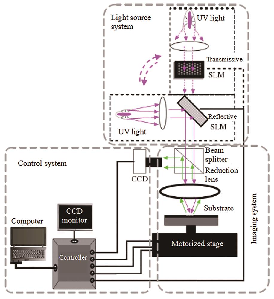
![Schematic illustration of SLM-based parallel micro/nano lithography system[12]](/richHtml/lop/2022/59/11/1100009/img_01.jpg)
Fig. 1. Schematic illustration of SLM-based parallel micro/nano lithography system[12]
![Principle and experimental results of multi-focus array produced by parallel micro/nano lithography. (a) Schematic diagram of multifocal modulation lithography system with spatial light modulator combined with micro-lens or zone plate array; (b) microstructure with characteristic size of 1.5 μm fabricated by multifocal parallel lithography[14]; (c) complex geometry and photonic devices fabricated by lithography[15]; (d) schematic diagram of holographic multifocal modulation lithography based on spatial light modulator; (e) schematic diagram of spiral photonic structure for parallel manufacturing of multifocal array, 45 focus fabricated “L” structure, 60 focus fabricated “Z” structure[18]](/richHtml/lop/2022/59/11/1100009/img_02.jpg)
Fig. 2. Principle and experimental results of multi-focus array produced by parallel micro/nano lithography. (a) Schematic diagram of multifocal modulation lithography system with spatial light modulator combined with micro-lens or zone plate array; (b) microstructure with characteristic size of 1.5 μm fabricated by multifocal parallel lithography[14]; (c) complex geometry and photonic devices fabricated by lithography[15]; (d) schematic diagram of holographic multifocal modulation lithography based on spatial light modulator; (e) schematic diagram of spiral photonic structure for parallel manufacturing of multifocal array, 45 focus fabricated “L” structure, 60 focus fabricated “Z” structure[18]
Fig. 3. Optimized processing by multifocal parallel micro/nano lithography. (a) Single focus,3 foci, 6 foci parallel manufacturing of sine curve structure diagram[26]; (b) formation of a 4×4 micrograph within 45 seconds[27]; (c) fabrication of same tissue scaffold structure using single beam and multiple beams[27]
Fig. 4. Principle of SLM-based direct projection micro-stereoscopic lithography[42]
Fig. 5. Microstructure formed by direct projection parallel lithography based on spatial light modulator. (a) Extracellular microenvironment was constructed, and four kinds of micro-pores were made on a single chip[54]; (b) stepwise; (c) spiral; (d) embryo-like; (e) flower-like; (f) micro-fans structure with 50 layers high and 10 μm thick; (g) micro-wineglass with 300 layers high and 4 μm thick[55]; (h) single micro-gear structure fabricated on hydrogel[58]
Fig. 6. Letters, triangle, and circles formed by linear holographic projection light field micro/nano lithography[59]
Fig. 7. Microstructure fabricated by modulating the incident light field into a “T” shaped light field, and the light source power is 560 mW. (a) 5 s; (b) 1 s; (c) 0.5 s; (d) 0.2 s[59]
Fig. 8. Incident light field is modulated into a uniform annular light field with controllable diameter, and the diameter is 25 μm tubular structure array, fabrication time is 15 s[60]
Fig. 9. Light field is modulated into circular, square, and triangular microstructure lithography results[59]. (a)‒(c) Lithography results before optimization; (d)‒(f) optimized lithography results
Fig. 10. Intensity distribution diagram when the beam is shaped into different patterns and the corresponding figure on DMD[64]. (a) Airy beam intensity distribution; (b) Bessel beam intensity distribution; (c) DMD display of the airy beam; (d) DMD display of the Bessel beam
Fig. 11. Cylindrical microstructure formed by Bessel beam lithography with different parameters[65]. (a) Hologram generating Bessel beam; (b) lithography results of cylindrical microstructure with different diameters
|
Table 1. Technical comparision of SLM-based parallel micro/nano lithography

Set citation alerts for the article
Please enter your email address


