• Chinese Optics Letters
  • Vol. 15, Issue 6, 062201 (2017)
Yonghui Zhang1、2, Zihui Zhang1、2, Chong Geng1、2, Shu Xu1、2, Tongbo Wei3、*, and Wen'gang Bi1、2
Author Affiliations
  • 1Institute of Micro-Nano Photoelectron and Electromagnetic Technology Innovation, School of Electronics and Information Engineering, Hebei University of Technology, Tianjin 300401, China
  • 2Key Laboratory of Electronic Materials and Devices of Tianjin, Tianjin 300401, China
  • 3Semiconductor Lighting Technology Research and Development Center, Institute of Semiconductors, Chinese Academy of Sciences, Beijing 100083, China
  • show less
    DOI: 10.3788/COL201715.062201 Cite this Article Set citation alerts
    Yonghui Zhang, Zihui Zhang, Chong Geng, Shu Xu, Tongbo Wei, Wen'gang Bi. Versatile nanosphere lithography technique combining multiple-exposure nanosphere lens lithography and nanosphere template lithography[J]. Chinese Optics Letters, 2017, 15(6): 062201 Copy Citation Text show less
    Process flowchart of MENSLL (Process A) and NSCL (Process B).
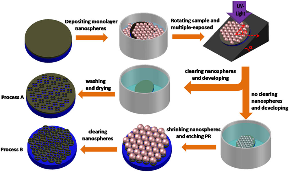
    Fig. 1. Process flowchart of MENSLL (Process A) and NSCL (Process B).
    (a) Simulated structure of FDTD; Electric field distributions for (b) 1200-nm-diameter nanosphere and (c) 600-nm-diameter nanosphere; Electric field distribution in XY plane for tilt exposure with the tilted angle (d) α=30°, (e) α=45°, (f) α=60°. Insets: Electric field distribution in XZ plane.
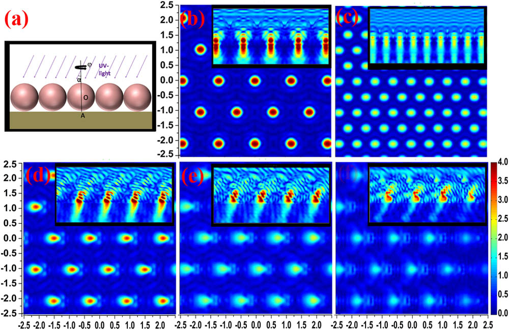
    Fig. 2. (a) Simulated structure of FDTD; Electric field distributions for (b) 1200-nm-diameter nanosphere and (c) 600-nm-diameter nanosphere; Electric field distribution in XY plane for tilt exposure with the tilted angle (d) α=30°, (e) α=45°, (f) α=60°. Insets: Electric field distribution in XZ plane.
    Plane-view SEM images for samples after (a) twin exposures when α=26.6° and ϕ=0°, 180°, (b) triple exposures when α=26.6° and ϕ=0°, 120°, 240°, (c) quadruple exposures when α=26.6° and ϕ=0°, 90°, 180°, 270°, (d) quintuple exposures when α=30° and ϕ=0°, 90°, 180°, 270°, and α=0° and ϕ=0°, (e) twin exposures when α=45° and ϕ=0°, 90°, (f) triple exposures when α=45° and ϕ=0°, 120°, 240°. The black scale bar is 4 μm.
    Fig. 3. Plane-view SEM images for samples after (a) twin exposures when α=26.6° and ϕ=0°, 180°, (b) triple exposures when α=26.6° and ϕ=0°, 120°, 240°, (c) quadruple exposures when α=26.6° and ϕ=0°, 90°, 180°, 270°, (d) quintuple exposures when α=30° and ϕ=0°, 90°, 180°, 270°, and α=0° and ϕ=0°, (e) twin exposures when α=45° and ϕ=0°, 90°, (f) triple exposures when α=45° and ϕ=0°, 120°, 240°. The black scale bar is 4 μm.
    SEM images of (a) the nanosphere monolayer after developing, (b) the nanosphere cleared partly, and (c) close-pack nanorings. The black scale bar is 2 μm.
    Fig. 4. SEM images of (a) the nanosphere monolayer after developing, (b) the nanosphere cleared partly, and (c) close-pack nanorings. The black scale bar is 2 μm.
    SEM images of nanring fabricated by shrinking silica spheres for (a) 180, (b) 270, and (c) 360 s. Insets: side view images. The black scale bar is 1 μm.
    Fig. 5. SEM images of nanring fabricated by shrinking silica spheres for (a) 180, (b) 270, and (c) 360 s. Insets: side view images. The black scale bar is 1 μm.
    SEM images of nanorescents fabricated in the conditions of (a) α=26.6° and shrinking silica spheres for 180 s, (b) α=45° and shrinking silica spheres for 180 s, and (c) α=26.6° and shrinking silica spheres for 270 s. Insets: side view images. The black scale bar is 1 μm.
    Fig. 6. SEM images of nanorescents fabricated in the conditions of (a) α=26.6° and shrinking silica spheres for 180 s, (b) α=45° and shrinking silica spheres for 180 s, and (c) α=26.6° and shrinking silica spheres for 270 s. Insets: side view images. The black scale bar is 1 μm.
    SEM images of hierarchical multiple structures with (b) triple exposures when α=26.6° and 0°, 120°, 240°, (c) quadruple exposures when α=26.6° and 0°, 90°, 180°, 270°, (d) quintuple exposures when α=26.6° and ϕ=0°, 72°, 144°, 216°, 288°. The black scale bar is 3 μm.
    Fig. 7. SEM images of hierarchical multiple structures with (b) triple exposures when α=26.6° and 0°, 120°, 240°, (c) quadruple exposures when α=26.6° and 0°, 90°, 180°, 270°, (d) quintuple exposures when α=26.6° and ϕ=0°, 72°, 144°, 216°, 288°. The black scale bar is 3 μm.
    Yonghui Zhang, Zihui Zhang, Chong Geng, Shu Xu, Tongbo Wei, Wen'gang Bi. Versatile nanosphere lithography technique combining multiple-exposure nanosphere lens lithography and nanosphere template lithography[J]. Chinese Optics Letters, 2017, 15(6): 062201
    Download Citation