Abstract
A versatile nanosphere composite lithography (NSCL) combining both the advantages of multiple-exposure nanosphere lens lithography (MENSLL) and nanosphere template lithography (NSTL) is demonstrated. By well controlling the development, washing and the drying processes, the nanosphere monolayer can be well retained on the substrate after developing and washing. Thus the NSTL can be performed based on MENSLL to fabricate nanoring, nanocrescent and hierarchical multiple structures. The pattern size and the shape can be systemically tuned by shrinking nanospheres by using dry etching and adjusting the tilted angle. It is a natural nanopattern alignment process and possesses a great potential in the scope of nano-science due to its low cost, simplicity, and versatility for variuos nano-fabrications.Nanotechnology has been growing rapidly in recent years and is becoming widely used in many fields of science and our daily life[1]. Generally, materials on a nanometer-scale possess unique properties due to their small length scales, low dimensionality, and interactions between neighboring particles[2]. The ability to conduct fabrications of the nanometer scale guarantees a continuing miniaturization of functional devices. Moreover, nanotechnology is expected to play a key role to find solutions to electronic, photonic, health care, or energy storage problems[3,4]. To further better develop nanoscience, various special nanopatterns are needed, such as nanoring[5], nanocrescents[6], nanocross[7], and nano cluster[8]. Most of conventional patterning methods cannot produce these special nanostructure arrays on substrates except electron-beam lithography[9]. However, electron-beam lithography is low in throughput and high in fabrication cost. Therefore, alternative and facile fabrication methods are needed to make nanostructures less expensive for the successful development of the nanotechnology.
A promising approach to fabricate well-ordered nanostructures is self-assembly nanosphere lithography (NSL) because of the simplicity and low cost[10–13]. According to the effect of nanosphere in lithography, NSL can be divided into nanosphere template lithography (NSTL) and nanosphere lens lithography (NSLL). The colloidal nanospheres usually assemble into hexagonal close-packed monolayer. On one hand, nanosphere arrays can be employed as templates for deposition or etching that can lead to the formation of other well-ordered nanostructures[14], which is called as NSTL. By NSTL, various nanopatterns such as nanocone[15], nanobowel[16], nanoring[17], nanocrescents[18], clover-shaped[19], hierarchical structural nanopore[20], and binary-structured arrays[21] have been fabricated. On the other hand, nanoshperes can be used as optical lenses to generate deep sub-wavelength regular patterns over large areas on a photoresist[22], which is called as NSLL. Nanohole[23], nanorod[24], 3D hierarchical architectures[25] have been fabricated by NSLL. Various nanopatterns can be fabricated by NSLL or NSTL, but they usually need to combine other complex technical such as tilted-rotary evaporation and ion beam milling. In addition, most NSL ways in references are NSTL or NSLL and only can be used to fabricate few patterns.
Here, we propose a versatile nanosphere composite lithography (NSCL) combining the multiple-exposure nanosphere lens lithography (MENSLL) and NSTL. It overcomes the disadvantages of low fill factor in normal NSLL. Furthermore, the lattice period, the fill factor and the gap between nanopatterns can be accurately tuned by adjusting the tilted angles, the rotated angles and the exposure times. Various special photoresist nanopatterns such as nanoring, nanocrescents, hierarchical multiple structures can be fabricated by NSCL. The attraction of our process is its low cost, large throughput, simplicity, and versatility for various nano-fabrications.
Sign up for Chinese Optics Letters TOC. Get the latest issue of Chinese Optics Letters delivered right to you!Sign up now
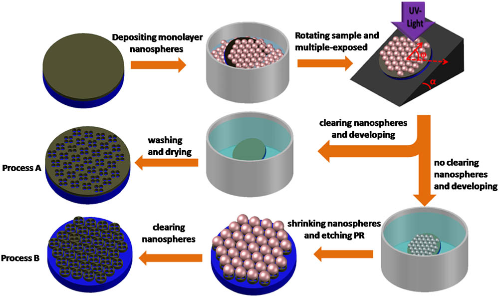
A detail process flowchart of multiple-exposure is shown in Fig. 1. The aqueous colloidal suspensions (typically 5 wt. %) were diluted with ethanol to form a 50 vol. % mixture of dispersion and ethanol. Then, the mixed colloidal suspensions were ultrasonic for 30 min to mix uniformitily. Microscopic glass slides with a thickness of 1 mm were cleaned by soaking in piranha solution (98% and 30% in a volume ratio) at room temperature for 30 min. After being rinsed with copious amount of DI water, they were dried by using stream before use. A part of the treated microscopic glass slide at a tilt angle of approximate 45° were inserted into the DI water in a rectangle glass dish with a width of 6 cm and length of 18 cm. The mixed colloidal suspension was carefully and uniformly dropped onto the top part of tilted glass slide. Once the suspension slides down to the interface of the water and the glass slide, the monolayer readily forms at the air–water interface. The mixed colloidal suspension continued to drop until the complete interface was covered by the monolayer. Then a drop of 2 wt. % SDS solution which could modify the water surface tension was added to consolidate the colloidal arrays into a large-area close-packed monolayer. A polymer resist (PR) was spin-coated onto the prepared substrate and prebaked at 95°C for 15 min. The measured thickness of the PR layer is 600 nm. Then the substrate was immersed into the subphase and elevated under a shallow angle to transfer the monolayer. The substrate was dried at an angle of approximately 45°. After drying, the substrates were put on a tilted base plate with angle. Then the wafer was rotated to different angles and the multiple-exposure was performed. The ultraviolet (UV) light power density is . Various nanopatterns can be obtained by combining different and values. As process A shows in Fig. 1, the multiple-exposed samples were developed at room temperature after clearing nanospheres. Immediately, the samples were put in the DI water and then blow-dryed with stream. 1200-nm-diameter PS sphere was used during the whole process A.

Figure 1.Process flowchart of MENSLL (Process A) and NSCL (Process B).
In addition, as NSCL (process B) shows in Fig. 1, samples with nanospheres can be immersed into developer after multiple exposures. Immediately, the samples were put in DI water for 2 s and then naturally dried in the air. The developed samples with nanospheres were dry-etched by inductively coupled plasma (ICP) with (40 sccm), Ar (40 sccm) and a bias power of 15 W for a certain time to tune the space of nanospheres. Then the (40 sccm) and a bias power of 40 W was used to etch PR for 100 s. Finally, the residual nanosphere monolayer was removed by blue adhesive tape or hydrofluoric acid.
To better understand the process, three dimensional finite difference time domain (3D-FDTD) is used to explore the optical characters of nanosphere lens. Figure 2(a) provides the simulated structure that is exposed to the UV light. Figures 2(b) and 2(c) show the simulation results for normal exposure using 1200-nm-diameter and 600-nm-diameter spheres. By comparing their electric field intensity, it can be found that the electric field intensity of forced spot is decreased with the decrease of nanosphere diameter. Therefore, it is necessary to increase the exposure time for small nanospheres so as to be completely exposed. In our experiments, the exposure times are set to 6 and 3 s for 600-nm and 1200-nm diameter spheres, respectively. Figures 2(d), 2(e), and 2(f) illustrate the simulated electric field energy distributions at , 45°, and 60° for nanospheres with 1200-nm diameter, respectively. Nanosphere still can focus light despite of the tilted light with different angles. The focused light spot shows the shape of circle for and abnormal oval away from nanosphere for other angles. As expected, the light spot is farther away from nanospheres with increasing . It is worth noting that electric field intensity is decreasing with increasing α. The main reason is that nanopheres harvest less light with the increasing due to the shadow effect of neighbor nanosphere. As a result, for the tilted exposure with large angles, a long exposure time is required to make PR fully exposed.
Figure 2.(a) Simulated structure of FDTD; Electric field distributions for (b) 1200-nm-diameter nanosphere and (c) 600-nm-diameter nanosphere; Electric field distribution in XY plane for tilt exposure with the tilted angle (d) , (e) , (f) . Insets: Electric field distribution in XZ plane.
Multiple and cross-shaped photoresist structures can be fabricated by simple MENSLL as process A shows in Fig. 1. Figure 3 shows SEM images of the various photoresist patterns fabricated by MENSLL with 1200-nm-diameter PS sphere. The angle is 26.6° for Figs. 3(a), 3(b), and 3(c). The exposure and the development times are 3 s and 2 s, respectively. Figure 3(a) shows the SEM image of the twin pattern exposure at (). The array of holes with square-like lattice can be obtained despite of the spheres with triangular lattice. Figure 3(b) shows the SEM image of the three-leaf clover pattern obtained using a triple exposure at (, 120°, 240°) while Fig. 3(c) shows the quadruple pattern obtained using quadruple exposure at (, 90°, 180°, 270°). Figure 3(d) shows the cross-shaped pattern obtained using quintuple exposure at ( and , 90°, 180°, 270°) and ( and ). The angle α is 45° for Figs. 3(e) and 3(f). The expose time is increased to 5 s because of the larger tilted angle. It can be seen in Fig. 3(e) that a hexagonal-like lattice can be obtained at (, 90°). Figure 3(f) shows the SEM image of holes with triangular lattice fabricated by the triple exposure at (, 120°, 240°). The lattice in Fig. 3(f) is different from that in Fig. 3(b) despite of the same because of the overlay of the holes produced by neighboring spheres at . Then holes with a larger diameter can be obtained. As shown above, MENSLL is able to fabricate a variable-shape periodic array such as multiple-pattern, cross-pattern, and other irregular patterns. For the MENSLL, the period size is equal to the nanosphere size, the arbitrary fill factor is available, and the pattern gap is controllable.
Figure 3.Plane-view SEM images for samples after (a) twin exposures when and , 180°, (b) triple exposures when and , 120°, 240°, (c) quadruple exposures when and , 90°, 180°, 270°, (d) quintuple exposures when and , 90°, 180°, 270°, and and , (e) twin exposures when and , 90°, (f) triple exposures when and , 120°, 240°. The black scale bar is 4 μm.
For MENSLL, it is difficult to fabricate ring-shape pattern. But in nano science field, the ring pattern is special important. Generally speaking, samples are developed after removing spheres in NSLL as process A shows in Fig. 1. Here, we develop the sample with nanosphere as process B shows in Fig. 1. It is well known that nanospheres will detach easily from the substrate at the substrate-water-air three phase contact line during immersion[26–28]. In our experiment, there are two critical points that make nanosphere monolayer not detach from the substrate at the substrate-water-air three phase contact line. First, it is necessary to fully dry samples in the air to enhance the interaction forces between nanosphere monolayer and PR, and also increase the adhesion among adjacent nanospheres. Second, the time during immersion into developer is extremely short, so there is no enough time for nanosphere monolayer to detach from the substrate at the substrate-water-air three phase contact line during immersion. After the development, the sample is immerged into water for only 2 s to wash the developer. Then the sample is dried in the air at the angle of approximate 45°. It is necessary to make nanospheres not fall off the substrate during washing after development. There are two different situations for nanospheres after development: (1) the PR that contacts nanosphes is not exposed. And the PR are intact after development, thus the nanosphere monolayer is intact on PR because of the interaction force between PR and nanospheres; (2) the PR that contacts nanospheres is fully exposed and etched after development. The nanosphere monolayer is intact on PR because the time during development and wash is too short for nanospheres to fall off the substrate. And the adhesive force between closed-packed nanospheres make the monolayer intact. During the natural drying in the air, it is easy for nanospheres to re-self-assemble in holes. Finally, the nanospheres are successfully retained on the substrate after development and washing. Then the surviving nanospheres are used as templates to drying etch the residual PR. Various ring patterns can be fabricated by combining MENSLL and NSTL. The silica spheres are used during the process because of its stability as template during ICP process. The exposure time is 6 and 3 s for 600-nm and 2000-nm silica spheres, respectively. The developing time is 3 s for all samples.
The SEM image in Fig. 4(a) shows that the 600-nm-diameter silica sphere monolayer exposed normally under UV-light is intact after developing and washing. To determine whether the PR under silica is developed, a part of silica sphere is lifted off by blue adhesive tape as shown in Fig. 4(b). It can be clearly seen that PR under spheres has been etched by developer and every silica sphere re-assembles in holes. The whole process is a natural nanopattern alignment process. Then is used to dry etch residual PR. Finally, the close-packed nanorings can be fabricated as shown in Fig. 4(c). It is obvious that the outer diameter of the ring is equal to the diameter of silica sphere, so it is also easy to tune the outer diameter of the ring by shrinking the size for silica spheres using ICP etching assisted with . Figure 5 shows the SEM imagines for nanorings with three different outer diameter values which are fabricated by shrinking silica spheres for 180, 270, and 360 s. The insets are the images for samples with partial nanospheres removed and the samples are placed with the tilted angle of 20°. The outer diameters are about 550, 530, 500 nm. The inner diameter is about 340 nm for all samples.
Figure 4.SEM images of (a) the nanosphere monolayer after developing, (b) the nanosphere cleared partly, and (c) close-pack nanorings. The black scale bar is 2 μm.
Figure 5.SEM images of nanring fabricated by shrinking silica spheres for (a) 180, (b) 270, and (c) 360 s. Insets: side view images. The black scale bar is 1 μm.
Furthermore, to fabricate nanocrescent, a sample is exposed when and , and 600-nm-diameter silica spheres is shrunk for 180 s. The fabricated nanocrescent is shown in Fig. 6(a). The process of fabricating nanocrescent is a subtraction boolean operation of nanopatterns. Namely, a big circle produced by scilica sphere as template substracts a small circle produced by scilica sphere as lens. The diameter of the big circle is equal to the diameter of the silica sphere. The position of the small circle is decided by the angle , so the shape of nanocrescents can be well controlled by the tilted angle and the diameter of scilica spheres. Figure 6(b) shows nanocrescents with smaller gap fabricated by exposing when and , and shrinking silica sphere for 180 s. Figure 6(c) shows a smaller nanocrescents fabricated by exposing when ° and , and shrinking silica sphere for 270 s.
Figure 6.SEM images of nanorescents fabricated in the conditions of (a) and shrinking silica spheres for 180 s, (b) and shrinking silica spheres for 180 s, and (c) and shrinking silica spheres for 270 s. Insets: side view images. The black scale bar is 1 μm.
Figure 7 provides the SEM images of hierarchical multiple structures fabricated by NSCL with 2000-nm-diameter scilica spheres when . Figure 7(a) shows the hierarchical three-leaf clover pattern obtained by conduction triple exposures sequentially at , 120°, 240°. Figure 7(b) shows the hierarchical quadruple patterns obtained by conducting quadruple exposures sequentially at , 90°, 180°, 270°. Figure 7(c) shows the hierarchical five-petals patterns obtained by using quintuple exposures sequentially at , 72°, 144°, 216, 228°.
Figure 7.SEM images of hierarchical multiple structures with (b) triple exposures when and 0°, 120°, 240°, (c) quadruple exposures when and 0°, 90°, 180°, 270°, (d) quintuple exposures when and , 72°, 144°, 216°, 288°. The black scale bar is 3 μm.
In conclusion, we demonstrate a versatile NSCL technique by combining MENSLL and NSTL to form various photoresist nanopatterns. By using MENSLL, various lattice structures such as triangle, square, hexagonal and multiple patterns arrays can be fabricated. The effect of the sphere diameter and the tilt angle of the light during exposure are explored by 3D-FDTD. Both small diameter and large tilted angle result in weak light intensity forced by nanosphere as lens. Furthermore, to fabricate nanoring, nanorescent and hierarchical multiple structure, the nanosphere monolayer is retained well on the substrate after developing and washing. The size of nanoring and nanorescent can be systemically controlled by shrinking nanospheres using ICP etching. This process is of low cost, simplicity, and versatility and possesses a great potential in nano-science field.
References
[1] Z. Dai, Y. Li, G. Duan, L. Jia, W. Cai. Acsnano, 6, 6706(2012).
[2] S. M. Yang, S. G. Jang, D. G. Choi, S. Kim, H. K. Yu. Small, 2, 458(2006).
[3] X. Zhao, B. M. Sanchez, P. J. Dobson, P. S. Grant. Nanoscale, 3, 839(2011).
[4] Y. Chen, Z. Li. Chin. Opt. Lett., 13, 020501(2015).
[5] J. Ye, J. A. Hutchison, H. Uji-i, J. Hofkens, L. Lagae, G. Maes, G. Borghs, P. Van Dorpe. Nanoscale, 4, 1606(2012).
[6] Z. A. Lewicka, Y. Li, A. Bohloul, W. W. Yu, V. L. Colvin. Nanotechnology, 24, 115303(2013).
[7] B. Ni, L. Huang, J. Ding, G. Li, X. Chen, W. Lu. Opt. Commun., 237, 298(2013).
[8] Z. Fang, Z. Liu, Y. Wang, P. M. Ajayan, P. Nordlander, N. J. Halas. Nano Lett., 12, 3808(2012).
[9] J. Cheng, N. Yan. Chin. Opt. Lett., 13, 082201(2015).
[10] C. L. Haynes, R. P. Duyne. J. Phys. Chem. B, 105, 5599(2001).
[11] J. Zhang, Y. Li, X. Zhang, B. Yang. Adv. Mater., 22, 4249(2010).
[12] X. Ye, L. Qi. Nano Today, 6, 608(2011).
[13] P. Zhu, N. Tansu. Photon. Res., 3, 184(2015).
[14] Z. A. Lewicka, A. Bahloul, W. W. Yu, V. L. Colvin. Nanoscale, 5, 11071(2013).
[15] A. Horrer, C. Schäfer, K. Broch, D. A. Gollmer, J. Rogalski, J. Fulmes, D. Zhang, A. J. Meixner, F. Schreiber, D. P. Kern, M. Fleischer. Small, 9, 3987(2013).
[16] X. D. Wang, E. Graugnard, J. S. King, Z. L. Wang, C. J. Summers. Nano Lett., 4, 2223(2004).
[17] Z. Li, P. Liu, Y. Liu, W. Chena, G. Wanga. Nanoscale, 3, 2743(2011).
[18] S. Cataldo, J. Zhao, F. Neubrech, B. Frank, C. Zhang, P. V. Braun, H. Giessen. Acsnano, 6, 979(2012).
[19] K. H. Li, Z. Ma, H. W. Choi. Appl. Phys. Lett., 100, 141101(2012).
[20] X. Wang, S. Xu, M. Cong, H. Li, Y. Gu, W. Xu. Small, 8, 972(2012).
[21] G. Liu, X. Li, W. Wang, F. Zhou, G. Duan, Y. Li, Z. Xu, W. Cai. Small, 10, 2374(2014).
[22] W. Wu, A. Katsnelson, O. G. Memis, H. Mohseni. Nanotechnology, 18, 485302(2007).
[23] Y. C. Chang, H. Ch. Chung, S. C. Lu, T. F. Guo. Nanotechnology, 24, 095302(2013).
[24] T. B. Wei, K. Wu, D. Lan, Q. F. Yan, Y. Chen, C. X. Du, J. X. Wang, Y. P. Zeng, J. M. Li. Appl. Phys. Lett., 101, 211111(2012).
[25] T. Y. Jeon, H. C. Jeon, S. Y. Lee, T. S. Shim, J. D. Kwon, S. G. Park, S. M. Yang. Adv. Mater., 26, 1422(2014).
[26] M. Retsch, Z. Zhou, S. Rivera, M. Kappl, X. S. Zhao, U. Jonas, Q. Li. Macromol. Chem. Phys., 210, 230(2009).
[27] Y. J. Zhang, W. Lib, K. J. Chen. J. Alloys Compd., 450, 512(2008).
[28] C. Geng, L. Zheng, J. Yu, Q. Yan, T. Wei, X. Wang, D. Shen. J. Mater. Chem., 22, 22678(2012).