• Journal of Semiconductors
  • Vol. 43, Issue 4, 042101 (2022)
Menglin Huang, Zhengneng Zheng, Zhenxing Dai, Xinjing Guo, Shanshan Wang, Lilai Jiang, Jinchen Wei, and Shiyou Chen
Author Affiliations
  • Key Laboratory of Computational Physical Sciences (MOE), and State Key Laboratory of ASIC and System, School of Microelectronics, Fudan University, Shanghai 200433, China
  • show less
    DOI: 10.1088/1674-4926/43/4/042101 Cite this Article
    Menglin Huang, Zhengneng Zheng, Zhenxing Dai, Xinjing Guo, Shanshan Wang, Lilai Jiang, Jinchen Wei, Shiyou Chen. DASP: Defect and Dopant ab-initio Simulation Package[J]. Journal of Semiconductors, 2022, 43(4): 042101 Copy Citation Text show less
    (Color online) The framework of the DASP software, which is composed of four modules, TSC, DEC, DDC and CDC. The major functions of the four modules are shown in the boxes.
    Fig. 1. (Color online) The framework of the DASP software, which is composed of four modules, TSC, DEC, DDC and CDC. The major functions of the four modules are shown in the boxes.
    (Color online) The flowchart of DASP. Different colors represent the four modules. The dashed lines show the calculations that need to call external ab-initio DFT software.
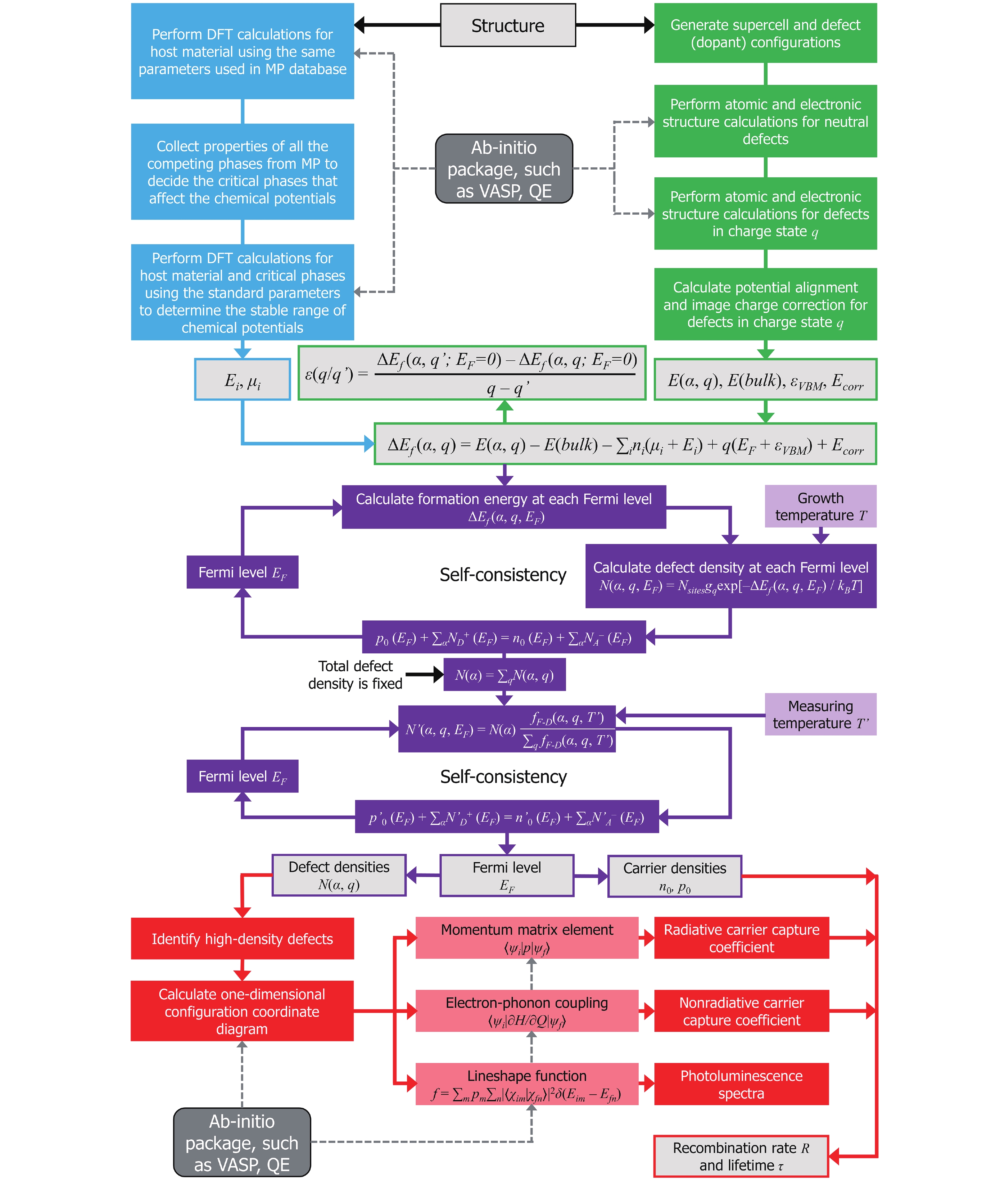
    Fig. 2. (Color online) The flowchart of DASP. Different colors represent the four modules. The dashed lines show the calculations that need to call external ab-initio DFT software.
    (Color online) The supercell generated by simple expansion of primitive cell and the maximumly-cubic supercell generated by DASP.
    Fig. 3. (Color online) The supercell generated by simple expansion of primitive cell and the maximumly-cubic supercell generated by DASP.
    (Color online) For a vacancy or antisite defect, the initial configuration (a) can be generated directly from the host lattice, and then structural perturbations are added, including (b) random displacements and (c) random distribution of the atoms within the sphere around the defect.
    Fig. 4. (Color online) For a vacancy or antisite defect, the initial configuration (a) can be generated directly from the host lattice, and then structural perturbations are added, including (b) random displacements and (c) random distribution of the atoms within the sphere around the defect.
    (Color online) The determination of the charge states of the ionized defect according to the calculated eigenvalues of the defect levels within the bulk band gap, extracted from the ab-initio calculation for the neutral defect.
    Fig. 5. (Color online) The determination of the charge states of the ionized defect according to the calculated eigenvalues of the defect levels within the bulk band gap, extracted from the ab-initio calculation for the neutral defect.
    (Color online) (a) Hole capture process by the donor defect D that changes the charge state from neutral to +1. (b) Configuration coordinate diagram of hole capture process. The potential curves are aligned to ensure the zero-phonon line energy equals to the (0/+) transition energy.
    Fig. 6. (Color online) (a) Hole capture process by the donor defect D that changes the charge state from neutral to +1. (b) Configuration coordinate diagram of hole capture process. The potential curves are aligned to ensure the zero-phonon line energy equals to the (0/+) transition energy.
    (Color online) Formation energies of point defects in GaN as functions of Fermi level under (a) Ga-rich and (b) N-rich conditions[54, 55].
    Fig. 7. (Color online) Formation energies of point defects in GaN as functions of Fermi level under (a) Ga-rich and (b) N-rich conditions[54, 55].
    (Color online) (a) Crystal structure, (b) band structure and density of states of SbSeI. (c) 3D and (d) projected-2D plot of phase stability diagram of SbSeI in the chemical potential space.
    Fig. 8. (Color online) (a) Crystal structure, (b) band structure and density of states of SbSeI. (c) 3D and (d) projected-2D plot of phase stability diagram of SbSeI in the chemical potential space.
    (Color online) Formation energies of point defects in SbSeI as functions of Fermi level under the chemical potential conditions (a) A, (b) B, (c) C, and (d) D.
    Fig. 9. (Color online) Formation energies of point defects in SbSeI as functions of Fermi level under the chemical potential conditions (a) A, (b) B, (c) C, and (d) D.
    (Color online) (a) The densities of defects in different charge states, electron and hole carrier densities and Fermi level as functions of the elemental chemical potentials. (b, c) The norm-squared wavefunctions of the neutral SeI and ISe defect states. (d) The charge-state transition levels of all defects in SbSeI.
    Fig. 10. (Color online) (a) The densities of defects in different charge states, electron and hole carrier densities and Fermi level as functions of the elemental chemical potentials. (b, c) The norm-squared wavefunctions of the neutral SeI and ISe defect states. (d) The charge-state transition levels of all defects in SbSeI.
    (Color online) (a) The location of (0/–) transition level of CN in the band gap of GaN. (b) Configuration coordinate diagram of the radiative transition of an electron from the CBM level to the (0/–) level of CN. (c) Calculated PL lineshape of CN at T = 300 K.
    Fig. 11. (Color online) (a) The location of (0/–) transition level of CN in the band gap of GaN. (b) Configuration coordinate diagram of the radiative transition of an electron from the CBM level to the (0/–) level of CN. (c) Calculated PL lineshape of CN at T = 300 K.
    Menglin Huang, Zhengneng Zheng, Zhenxing Dai, Xinjing Guo, Shanshan Wang, Lilai Jiang, Jinchen Wei, Shiyou Chen. DASP: Defect and Dopant ab-initio Simulation Package[J]. Journal of Semiconductors, 2022, 43(4): 042101
    Download Citation