
Yaozheng Wu, Bin Liu, Feifan Xu, Yimeng Sang, Tao Tao, Zili Xie, Ke Wang, Xiangqian Xiu, Peng Chen, Dunjun Chen, Hai Lu, Rong Zhang, Youdou Zheng. High-efficiency green micro-LEDs with GaN tunnel junctions grown hybrid by PA-MBE and MOCVD[J]. Photonics Research, 2021, 9(9): 1683
- Photonics Research
- Vol. 9, Issue 9, 1683 (2021)
Abstract
1. INTRODUCTION
Owing to their high luminous efficiency, chemical stability, and long lifetime, GaN-based LEDs are widely used in solid-state lighting and displays. Compared with traditional LEDs, the size of micro-LEDs can be decreased to tens of micrometers, and each pixel can be controlled or driven independently, which has achieved many advantages in high-resolution displays and visible-light communication (VLC) [1–5]. The outstanding performance of blue micro-LEDs has already been demonstrated in VLC. However, realizing long-wavelength emission for InGaN micro-LEDs is still challenging due to the severe efficiency droop, with the indium content increasing in the InGaN layer. Besides, GaN epi-layers with high crystal quality and low p-type conductivity are still hard to realize due to high activation energy for Mg, which results in insufficient current spreading and low hole injection efficiency.
Tunnel junction (TJ) is an effective way to enhance hole injection and reduce the sheet resistance of GaN-based optoelectronic devices [6,7]. The TJ diode generally requires highly doped as the interface of a p-n junction. The electrons may tunnel from the valence band of to the conduction band of at a specific reverse bias voltage, and finally result in hole injection into the active region effectively [8]. The introduction of TJ makes on both ends of the device n-type GaN layers with relatively low resistance. This effectively avoids the p-type contact difficulty in traditional LED devices and finally simplifies the device-fabrication process. Besides, the preparation of TJ increases the lateral current spreading and achieves uniform optical output and relatively low forward turn-on voltage. It not only prevents the additional optical loss compared with a traditional transparent current spreading layer such as indium tin oxide (ITO), but also avoids the influence of high ITO growth temperature on the crystal quality of the active region [9,10].
The realization of a GaN-based homo-junction for tunneling is still challenging due to the low direct band-to-band tunneling probability owing to its wide bandgap. Several groups have tried to introduce a thin InGaN or AlN polarization dipole layer to shrink the width of the depletion region [11–14]. Although the n-type GaN with high electron concentration above can be achieved by Si or Ge doping, the highly doped p-GaN is still difficult to prepare by metal–organic chemical vapor deposition (MOCVD) owing to hydrogen passivation [15–17]. Besides, it is difficult to fabricate TJs by MOCVD because the buried p-GaN below a highly doped n-GaN is not easy to be activated due to the difficult diffusion of hydrogen atoms [18,19]. Further, Mg memory effects may lead to impurity compensation in the n-GaN layer and finally enlarged depletion width [20,21]. On the contrary, the absence of hydrogen introduction during growth by molecular beam epitaxy (MBE) makes it an ideal technique for the fabrication of devices with TJs [22–25].
Sign up for Photonics Research TOC. Get the latest issue of Photonics Research delivered right to you!Sign up now
In this work, we report on the realization of high-efficiency green micro-LEDs with GaN-based TJs grown hybrid by plasma-assisted MBE (PA-MBE) and MOCVD. As shown in Fig. 1(a), the epi-wafer structures can be divided into two parts: a standard LED structure fabricated by MOCVD and an ultra-thin unintentionally doped (UID) InGaN polarization layer as well as an layer prepared by PA-MBE.
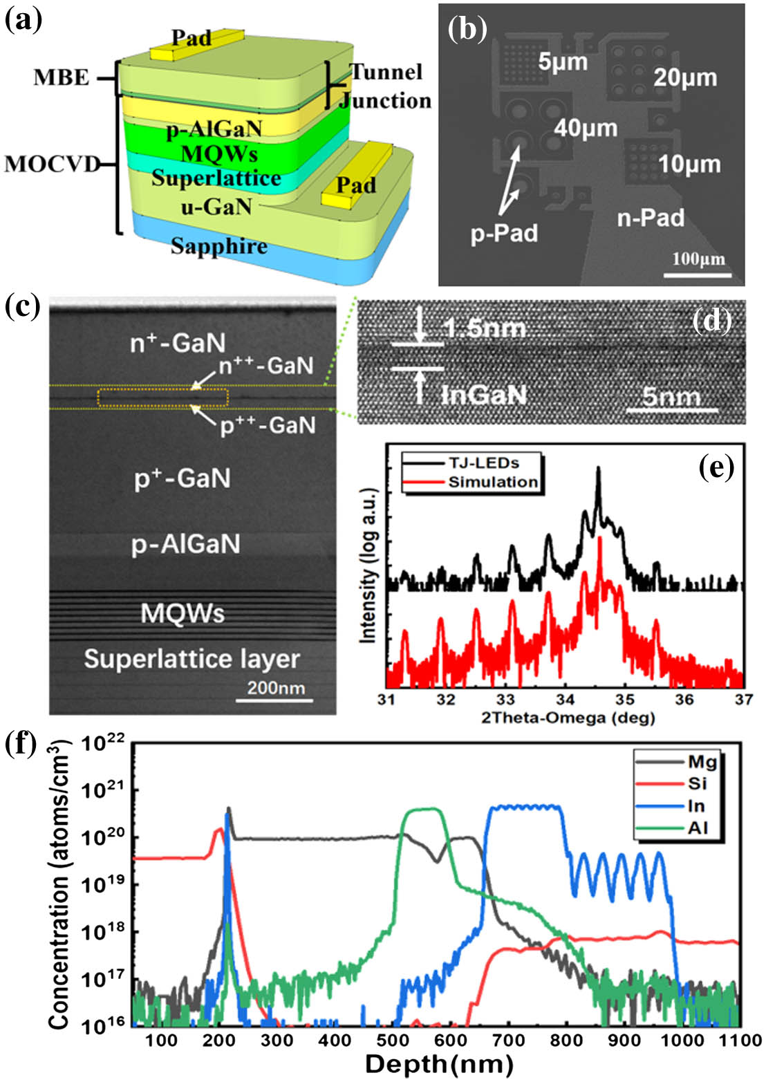
Figure 1.(a) Schematic diagram of the TJ micro-LED. (b) Top view SEM images of TJ micro-LEDs. (c) and (d) TEM images of TJ LED structure and InGaN polarization layer. (e) Experimental and simulated XRD scans along (0002) direction. (f) Depth profiles of Si, Mg, In, and Al concentrations of the TJ LED measured by SIMS.
2. EXPERIMENT
The standard LED structure was grown on patterned c-plane sapphire substrates and consists of a UID-GaN template layer, a Si-doped n-GaN layer, a six-period Si-doped super-lattice layer proposed to release the stress in active region and reduce quantum-confined Stark effect (QCSE) effects, an active region with nine-period MQWs with photoluminescence (PL) emission wavelength of 530 nm, an AlGaN electron-blocking layer (EBL), and a Mg-doped layer with a thin () as a contact layer. After the MOCVD growth, the epi-wafer was annealed effectively to activate the p-type layer. Before the MBE regrowth, a treatment by hydrofluoric acid was needed to remove the residual O and Mg on the LED epi-wafer surface [22]. The standard LED epi-wafer was then loaded into the MBE chamber to regrow an ultra-thin UID InGaN layer, a 30 nm layer, and a 200 nm layer. The surface preparation and the dislocation control at the regrowth interface have been studied in our previous work [26]. According to the transmission electron microscopy (TEM) images in Figs. 1(c) and 1(d), the thicknesses of the InGaN quantum well (QW) and GaN quantum barrier (QB) were measured to be 3 and 12 nm, respectively. The clear and sharp interfaces of each layer were shown intuitively, which manifest that the crystalline quality of InGaN QWs was not found to deteriorate after the regrowth processes. The thickness of the InGaN polarization layer was around 1.5 nm, and no new dislocations were generated at the regrowth interface. As illustrated in Fig. 1(e), the strong intensity of satellite peaks of InGaN/GaN MQWs can be seen clearly, which indicates the sharp MQWs interface and the good crystal quality after regrowth. The secondary ion mass spectroscopy (SIMS) profiles were shown in Fig. 1(f). The concentrations of silicon and magnesium in the and TJ layers were and , respectively, while in the and layer were and , respectively. At the interface of the TJ layer, the concentration of Mg dopant decreased sharply at the side of the layer owing to the avoidance of the Mg memory effect with the PA-MBE regrowth processes, which guaranteed the high electron and hole concentration distributed at the and layer, respectively.
For device fabrication, 200 nm thick mask layers both with and without TJ epi-wafers were firstly deposited by plasma-enhanced chemical vapor deposition (PECVD) and then transformed into micro-pillar pixel arrays with the depth of 1.2 μm and different diameters of 40, 20, 10, and 5 μm by standard contact photolithography, reactive ion etching (RIE), and inductively coupled plasma (ICP) etching processes. The mask layer was then removed by buffered oxide etching (BOE) solution. Next, a 200 nm thick passivation layer was deposited onto both samples by PECVD after wet chemical surface treatment by potassium hydroxide (KOH) and nitric acid (). The metal contact windows were chemically etched by RIE processes. To simplify the electrode fabrication processes, the n-/p-type metal contact (Cr/Au, 50 nm/150 nm) for both TJ and standard micro-LED samples was deposited on the corresponding region. The top-view SEM images of TJ micro-LEDs are shown in Fig. 1(b).
3. RESULTS AND DISCUSSION
In order to study the influence of device size on their optical performance, room-temperature μ-PL and time-resolved PL (TR-PL) measurements were taken into consideration and the results are shown in Fig. 2. Samples were excited by a 375 nm diode laser and the laser spot was focused onto the sample with a diameter of 2 μm. The luminescence signals were collected by a Horiba iHR320 monochromator and detected by a Synapse CCD detector. While in the measurement of time-resolved PL (TRPL), the signal was collected by a time-correlated single-photon counting system (TCSPC) with a time resolution of 50 ps. It can be seen from Fig. 2(a) that the intensity of μ-PL spectra is enhanced significantly as the size of the devices decreased from 40 to 5 μm. The enhanced μ-PL spectral intensity cannot be owing to the diminished polarization field cause by strain relaxation in the active region, because the blueshift of the μ-PL emission peak was not found in the measurements. On the contrary, we were inclined to believe that the Purcell effect may play an important role in this phenomenon owing to the reduced optical cavity size. In fact, the enhancement factor can be described as follows [27]:
![]()
Figure 2.(a) Enhanced PL spectra with different device size. (b) Normalized TR-PL spectra of designed TJ micro-LEDs with different device size. Inset shows the relationship between
The current density versus voltage characterizations of standard LEDs and TJ-LEDs with a diameter of 40 μm was examined by a Lakeshore probe system equipped with liquid helium cycle refrigeration and a Keithley 2636 Digital source-meter; the results are shown in Fig. 3(a). The turn-on voltage of the TJ micro-LEDs was estimated to be around 2.9 V, smaller than that of the standard micro-LED structure. By fitting the linear regime (3.4–4 V) of the I-V curves, the total resistance of TJ micro-LEDs () is significantly lower than that of normal structure micro-LEDs (). The reason can be explained by the perfect current spreading performance and enhanced hole injection efficiency of the TJ-LED structure. For a detailed study of the difference between TJ micro-LEDs and standard micro-LEDs, the J-V curves were converted to logarithmic coordinate. The test scope was divided into regions I, II, and III according to the working state of the LEDs. In region I, the reverse electrical leakage current of these two kinds of micro-LED structures has a good coincidence and remained at a low magnitude. In region II, where the applied forward voltage is smaller than the tunneling voltage, the leakage current density of the TJ micro-LEDs showed a lower magnitude than that of standard micro-LEDs. It can be concluded that the reason for this is the low tunneling rate hampered the forward electrical leakage current of the sub-standard micro-LED structure. In region III, when the applied forward voltage is higher than the tunneling voltage, the forward current density of TJ micro-LEDs increased dramatically and finally became higher than that of standard micro-LEDs. In this case, it is believed that the TJs are operated at the tunneling voltage with a high tunneling rate and provide a high magnitude of the hole for current injection [12].
![]()
Figure 3.(a) Room temperature
To further explore the electrical properties of TJ micro-LEDs under the forward bias, I-V characteristics with temperature ranging from 10 to 290 K were gathered and the results are shown in Fig. 3(b). Unlike standard LEDs, it can be seen that the J-V curves in region II showed no change under varied temperature and the forward leakage current remained at a low level, which indicated inter-band tunneling as the transport mechanism in such TJs. The TJs behave like a Zener tunneling diode, which shows a strong backward diode behavior with a much higher current and weak temperature dependence at reverse bias than at forward bias [29–31]. Moreover, when the forward bias increased until the devices worked at region III, the J-V characterization showed strong temperature dependence. This indicated that the high current density of inter-band tunneling is realized in this region. The performance of the device was the same as that of a standard LED. In fact, the TJs act as a “switch” which showed an “OFF” status in region II and an “ON” status in region III. However, at the boundary of regions II and III, the devices showed strong temperature dependence and decreased from 2.0 V at 10 K to 1.6 V at 290 K. In this area, although the tunneling rate is relatively low, the magnitude of electrical leakage current due to the forward bias is influenced by temperature markedly and therefore shows a higher current measurement with an increased temperature.
As shown in Fig. 4(a), the room temperature electroluminescence (EL) spectra of single-pixel TJ micro-LEDs with the diameter of 40 μm were measured at current density ranging from to , and the peak emission wavelength showed a blueshift of around 12 nm, mainly attributed to the polarization-related quantum-confined Stark effect (QCSE) in the MQWs. The optical micrograph of the TJ micro-LEDs tested at is also shown in the inset. The relationship between the injection current and the EL density of the two kinds of micro-LED structures manifests that the TJ micro-LEDs showed a better luminescent property at high current injection than standard micro-LEDs. The dependence of the normalized EQE on the current density of both two kinds of micro-LEDs is shown in Fig. 4(b). At the current density of , the normalized EQEs of TJ and standard micro-LEDs were 75% and 53%, respectively. Besides, the peak of normalized EQE of TJ micro-LEDs is around , slightly smaller than that of standard micro-LEDs, which is around . The normalized EQE peak of TJ micro-LEDs was gentler than that of the standard one. Moreover, the TJ micro-LEDs showed a higher EQE than the reference LEDs and can be lighted at an even lower injection current density. The reduced efficiency droop and lower injection current density for luminescence may be attributed to the enhanced hole injection rate, which finally increased the wave function overlap of electrons and holes even at a low injection current density. This also may be owing to the improved current spreading uniformity in , which may reduce the current crowding effect [32,33]. In fact, according to the ABC model, EQE can be expressed as follows:
![]()
Figure 4.(a) EL intensity of two samples with device diameter of 40 μm. Inset shows the EL intensity of TJ micro-LEDs with the current density ranging from
The influence of size reduction on the performances of TJ micro-LEDs was also studied with the diameters of 40, 20, 10 and 5 μm. For better device performances, the n-type metal contact (Ti/Al/Ni/Au, 30/150/50/100 nm) was deposited on the n-pad region and then annealed at 850°C in nitrogen atmosphere for Ohmic contact. The current density as a function of applied voltage for different device size is shown in Fig. 5(a). Unlike the J-V characteristics of traditional micro-LEDs [34,35], one can clearly see that the current densities were independent of device size when the applied forward voltage was higher than the threshold voltage, which is valid evidence for the high performance of current spreading efficiency with TJs. However, when below the threshold voltage, the forward leakage current showed a strong dependence on the size of device. The leakage current increased parallel with the size of device decreasing from 40 to 5 μm, which indicated that the increased leakage current was not leaked from the bulk of TJs but the sidewall defects caused by dry etching [36]. The normalized EQE of micro-LEDs with different device size is represented as a function of current density in Fig. 5(b). It is obvious that the normalized EQE depends on the size of device. Smaller LEDs achieve their maximum EQE at a higher current density and show a reduced efficiency droop at high injection current density. Besides, in a logarithmic scale, the onset of EQE tends to move towards high current densities as the size of device decreases to 5 μm. The surface recombination effect on the sidewalls may play an important role in this onset transition due to the increased surface/bulk ratio [37,38]. The defect-related non-radiative recombination coefficient, , can be described as follows [36,39]:
![]()
Figure 5.(a)
4. CONCLUSIONS
In summary, we fabricated GaN-based TJs on traditional green LED epi-wafers by PA-MBE to increase the hole injection rate. No new dislocations were observed at the regrowth interface. The steep doping interface was measured with SIMS, which may result in ultrathin depletion width for efficient inter-band tunneling. The as-prepared epi-wafers were fabricated into micro-LEDs with different sizes. Compared with standard micro-LEDs, TJ micro-LEDs showed a reduced device resistance, enhanced EL intensity, and a reduced efficiency droop. The size-independent J-V characteristics of the green TJ micro-LED also revealed that the MBE-grown served as a uniform current spreading layer, which paves the way for the fabrication of high-performance micro-LEDs.
References
[1] K. Zhang, D. Peng, K. M. Lau, Z. J. Liu. Fully-integrated active matrix programmable UV and blue micro-LED display system-on-panel (SoP). J. Soc. Inf. Disp., 25, 240-248(2017).
[2] T. Z. Wu, C. W. Sher, Y. Lin, C. F. Lee, S. J. Liang, Y. J. Lu, C. S. W. Huang, W. J. Guo, H. C. Kuo, Z. Chen. Mini-LED and micro-LED: promising candidates for the next generation display technology. Appl. Sci., 8, 1557(2018).
[3] M. D. Dawson, J. J. D. McKendry, Z. Gong, E. Gu, A. E. Kelly, D. Massoubre, R. P. Green, B. Guilhaber. High-speed visible light communications using individual pixels in a micro light-emitting diode array. IEEE Photon. Technol. Lett., 22, 1346-1348(2010).
[4] P. F. Tian, X. Y. Liu, S. Y. Yi, Y. X. Huang, S. L. Zhang, X. L. Zhou, L. G. Hu, L. R. Zheng, R. Liu. High-speed underwater optical wireless communication using a blue GaN-based micro-LED. Opt. Express, 25, 1193-1201(2017).
[5] J. Y. Lin, H. X. Jiang. Development of microLED. Appl. Phys. Lett., 116, 100502(2020).
[6] S. Neugebauer, M. P. Hoffmann, H. Witte, J. Bläsing, A. Dadgar, A. Strittmatter, T. Niermann, M. Narodovitch, M. Lehmann. All metalorganic chemical vapor phase epitaxy of p/n-GaN tunnel junction for blue light emitting diode applications. Appl. Phys. Lett., 110, 102104(2017).
[7] S. Krishnamoorthy, F. Akyol, P. S. Park, S. Rajan. Low resistance GaN/InGaN/GaN tunnel junctions. Appl. Phys. Lett., 102, 113503(2013).
[8] L. Esaki. New phenomenon in narrow germanium p–n junctions. Phys. Rev., 109, 603-604(1958).
[9] J. T. Leonard, D. A. Cohen, B. P. Yonkee, R. M. Farrell, T. Margalith, S. Lee, S. P. DenBaars, J. S. Speck, S. Nakamura. Nonpolar III-nitride vertical-cavity surface emitting lasers incorporating an ion implanted aperture. Appl. Phys. Lett., 107, 011102(2015).
[10] M. T. Hardy, C. O. Holder, D. F. Feezell, S. Nakamura, J. S. Speck, D. A. Cohen, S. P. DenBaars. Indium-tin-oxide clad blue and true green semipolar InGaN/GaN laser diodes. Appl. Phys. Lett., 103, 081103(2013).
[11] C. Lund, B. Romanczyk, M. Catalano, Q. X. Wang, W. J. Li, D. DiGiovanni, M. J. Kim, P. Fay, S. Nakamura, S. P. DenBaars, U. K. Mishra, S. Keller. Metal-organic chemical vapor deposition of high quality, high indium composition N-polar InGaN layers for tunnel devices. J. Appl. Phys., 121, 185707(2017).
[12] X. D. Yan, W. J. Li, S. M. Islam, K. Pourang, H. L. Xing, P. Fay, D. Jena. Polarization-induced Zener tunnel diodes in GaN/InGaN/GaN heterojunctions. Appl. Phys. Lett., 107, 163504(2015).
[13] S. Krishnamoorthy, P. S. Park, S. Rajan. Demonstration of forward inter-band tunneling in GaN by polarization engineering. Appl. Phys. Lett., 99, 233504(2011).
[14] J. Simon, Z. Zhang, K. Goodman, H. L. Xing, T. Kosel, P. Fay, D. Jena. Polarization-induced Zener tunnel junctions in wide-band-gap heterostructures. Phys. Rev. Lett., 103, 026801(2009).
[15] E. Richter, T. Stoica, U. Zeimer, C. Netzel, M. Weyers, G. Tränkle. Si doping of GaN in hydride vapor-phase epitaxy. J. Electron. Mater., 42, 820-825(2013).
[16] S. Fritze, A. Dadgar, H. Witte, M. Bügler, A. Rohrbeck, J. Bläsing, A. Hoffmann, A. Krost. High Si and Ge n-type doping of GaN doping—limits and impact on stress. Appl. Phys. Lett., 100, 122104(2012).
[17] A. Hierro, S. A. Ringel, M. Hansen, J. S. Speck, U. K. Mishra, S. P. DenBaars. Hydrogen passivation of deep levels in n–GaN. Appl. Phys. Lett., 77, 1499-1501(2000).
[18] A. Y. Polyakov, N. B. Smirnov, S. J. Pearton, F. Ren, B. Theys, F. Jomard, Z. Teukam, V. A. Dmitriev, A. E. Nikolaev, A. S. Usikov, I. P. Nikitina. Fermi level dependence of hydrogen diffusivity in GaN. Appl. Phys. Lett., 79, 1834-1836(2001).
[19] J. Neugebauer, C. G. Van de Walle. Role of hydrogen in doping of GaN. Appl. Phys. Lett., 68, 1829-1831(1996).
[20] Y. Kuwano, M. Kaga, T. Morita, K. Yamashita, K. Yagi, M. Iwaya, T. Takeuchi, S. Kamiyama, I. Akasaki. Lateral hydrogen diffusion at p-GaN layers in nitride-based light emitting diodes with tunnel junctions. Jpn. J. Appl. Phys., 52, 08JK12(2013).
[21] T. Takeuchi, G. Hasnain, S. Corzine, M. Hueschen, R. P. Schneider, C. Kocot, M. Blomqvist, Y. Chang, D. Lefforge, M. R. Krames, L. W. Cook, S. A. Stockman. GaN-based light emitting diodes with tunnel junctions. Jpn. J. Appl. Phys., 40, L861-L863(2001).
[22] B. P. Yonkee, E. C. Young, S. P. Denbaars, S. Nakamura, J. S. Speck. Silver free III-nitride flip chip light-emitting-diode with wall plug efficiency over 70% utilizing a GaN tunnel junction. Appl. Phys. Lett., 109, 191104(2016).
[23] E. C. Young, B. P. Yonkee, F. Wu, S. H. Oh, S. P. DenBaars, S. Nakamura, J. S. Speck. Hybrid tunnel junction contacts to III–nitride light-emitting diodes. Appl. Phys. Express, 9, 022102(2016).
[24] J. T. Leonard, E. C. Young, B. P. Yonkee, D. A. Cohen, T. Margalith, S. P. DenBaars, J. S. Speck, S. Nakamura. Demonstration of a III-nitride vertical-cavity surface-emitting laser with a III-nitride tunnel junction intracavity contact. Appl. Phys. Lett., 107, 091105(2015).
[25] M. Malinverni, D. Martin, N. Grandjean. InGaN based micro light emitting diodes featuring a buried GaN tunnel junction. Appl. Phys. Lett., 107, 051107(2015).
[26] Y. Z. Wu, B. Liu, Z. H. Li, T. Tao, Z. L. Xie, X. Q. Xiu, P. Chen, D. J. Chen, H. Lu, Y. Shi, R. Zhang, Y. D. Zheng. Homo-epitaxial growth of high crystal quality GaN thin films by plasma assisted–molecular beam epitaxy. J. Cryst. Growth, 506, 30-35(2019).
[27] R. Baets, D. Delbeke, R. Bockstaele, P. Bienstman. Resonant-cavity light-emitting diodes: a review. Proc. SPIE, 4996, 74-86(2003).
[28] S. F. Chichibu, K. Hazu, Y. Ishikawa, M. Tashiro, H. Namita, S. Nagao, A. Uedono. Time-resolved photoluminescence, positron annihilation, and Al0.23Ga0.77N/GaN heterostructure growth studies on low defect density polar and nonpolar freestanding GaN substrates grown by hydride vapor phase epitaxy. J. Appl. Phys., 111, 103518(2012).
[29] X. D. Yan, W. J. Li, S. M. Islam, K. Pourang, H. Xing, P. Fay, D. Jena. Polarization-induced Zener tunnel diodes in GaN/InGaN/GaN heterojunctions. Appl. Phys. Lett., 107, 163504(2015).
[30] S. Krishnamoorthy, D. N. Nath, F. Akyol, P. S. Park, M. Esposto, S. Rajan. Polarization-engineered GaN/InGaN/GaN tunnel diodes. Appl. Phys. Lett., 97, 203502(2010).
[31] J. Simon, Z. Zhang, K. Goodman, H. Xing, T. Kosel, P. Fay, D. Jena. Polarization-induced Zener tunnel junctions in wide-band-gap heterostructures. Phys. Rev. Lett., 103, 026801(2009).
[32] V. K. Malyutenko, S. S. Bolgov, A. D. Podoltsev. Current crowding effect on the ideality factor and efficiency droop in blue lateral InGaN/GaN light emitting diodes. Appl. Phys. Lett., 97, 251110(2010).
[33] S. Huang, B. Fan, Z. Chen, Z. Zheng, H. Luo, Z. Wu, G. Wang, H. Jiang. Lateral current spreading effect on the efficiency droop in GaN based light-emitting diodes. J. Disp. Technol., 9, 266-271(2013).
[34] K. Zhang, Y. B. Liu, H. S. Kwok, Z. J. Liu. Investigation of electrical properties and reliability of GaN-based micro-LEDs. Nanomaterials, 10, 689(2020).
[35] Z. Gong, S. R. Jin, Y. J. Chen, J. McKendry, D. Massoubre, I. M. Watson, E. Gu, M. D. Dawson. Size-dependent light output, spectral shift, and self-heating of 400 nm InGaN light-emitting diodes. J. Appl. Phys., 107, 013103(2010).
[36] J. M. Smith, R. Ley, M. S. Wong, Y. H. Baek, J. H. Kang, C. H. Kim, M. J. Gordon, S. Nakamura, J. S. Speck, S. P. DenBaars. Comparison of size-dependent characteristics of blue and green InGaN microLEDs down to 1 μm in diameter. Appl. Phys. Lett., 116, 071102(2020).
[37] P. Tian, J. J. D. McKendry, Z. Gong, B. Guilhabert, I. M. Watson, E. Gu, Z. Chen, G. Zhang, M. D. Dawson. Size-dependent efficiency and efficiency droop of blue InGaN micro-light emitting diodes. Appl. Phys. Lett., 101, 231110(2012).
[38] S. S. Konoplev, K. A. Bulashevich, S. Y. Karpov. From large-size to micro-LEDs: scaling trends revealed by modeling. Phys. Status Solidi A, 215, 1700508(2017).
[39] K. A. Bulashevich, S. Y. Karpov. Impact of surface recombination on efficiency of III-nitride light-emitting diodes. Phys. Status Solidi RRL, 10, 480-484(2016).

Set citation alerts for the article
Please enter your email address
© Copyright 2018-2021 | Chinese Laser Press. All Rights Reserved 沪ICP备15018463号-20