• Opto-Electronic Advances
  • Vol. 1, Issue 4, 180007-1 (2018)
Zhixin Liu, Meiling Jiang, Yanglin Hu, Feng Lin, Bo Shen, Xing Zhu, and Zheyu Fang*
Author Affiliations
  • School of Physics, State Key Lab for Mesoscopic Physics, Academy for Advanced Interdisciplinary Studies, Collaborative Innovation Center of Quantum Matter, Peking University, Beijing 100871, China
  • show less
    DOI: 10.29026/oea.2018.180007 Cite this Article
    Zhixin Liu, Meiling Jiang, Yanglin Hu, Feng Lin, Bo Shen, Xing Zhu, Zheyu Fang. Scanning cathodoluminescence microscopy: applications in semiconductor and metallic nanostructures[J]. Opto-Electronic Advances, 2018, 1(4): 180007-1 Copy Citation Text show less
    Schematic overview of a CL imaging spectrometer with spectral analysis function.Figure reproduced from ref. 11, CUP Publishing.
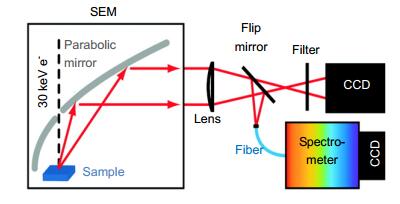
    Fig. 1. Schematic overview of a CL imaging spectrometer with spectral analysis function.Figure reproduced from ref. 11, CUP Publishing.
    (a) SEM image of the GaN/InGaN multiple quantum well surface. (b, c) CL image of the same area of (a) at electron beam currents of 0.11 nA and 3.73 nA, respectively. (d–f) The same images at lower magnification clearly demonstrate the decline in luminous efficiency.Figure reproduced from ref. 56, AIP Publishing.
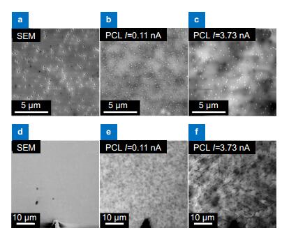
    Fig. 2. (a) SEM image of the GaN/InGaN multiple quantum well surface. (b, c) CL image of the same area of (a) at electron beam currents of 0.11 nA and 3.73 nA, respectively. (d–f) The same images at lower magnification clearly demonstrate the decline in luminous efficiency.Figure reproduced from ref. 56, AIP Publishing.
    (a) Schematic of CL method for the measurement of Ld. (b)Ld as a function of the electron-beam current ib at 5 K. Inset: Schematic of the carrier transport in conjunction with localized states for low (ⅰ) and high (ⅱ) densities of localized states.Figure reproduced from ref. 57, John Wiley & Son.
    Fig. 3. (a) Schematic of CL method for the measurement of Ld. (b)Ld as a function of the electron-beam current ib at 5 K. Inset: Schematic of the carrier transport in conjunction with localized states for low (ⅰ) and high (ⅱ) densities of localized states.Figure reproduced from ref. 57, John Wiley & Son.
    (a) Schematic, CL images and SEM image of the single nanocolumn. (b) CL spectra of two single GaN/AlGaN nanocolumns.Figure reproduced from ref. 59, AIP Publishing.
    Fig. 4. (a) Schematic, CL images and SEM image of the single nanocolumn. (b) CL spectra of two single GaN/AlGaN nanocolumns.Figure reproduced from ref. 59, AIP Publishing.
    (a) Schematic of the electron beam interaction with nanowire and luminescence emission. (b) SEM image of a single nanowire. (c) CL image of a single GaAs nanowire measured at 30 K. (d) CL spectrum from nanowire at room temperature and the fit (red curve).Figure reproduced from ref. 54, ACS Publications.
    Fig. 5. (a) Schematic of the electron beam interaction with nanowire and luminescence emission. (b) SEM image of a single nanowire. (c) CL image of a single GaAs nanowire measured at 30 K. (d) CL spectrum from nanowire at room temperature and the fit (red curve).Figure reproduced from ref. 54, ACS Publications.
    (a) Schematic of hBN/WSe2/hBN van der waals heterojunction excited by electron beam. (b) Process of the generation, diffusion, and recombination of electron−hole (e-h) pairs in heterojunction. (c) Optical microscope image of a hBN/ WSe2/hBN heterostructure. (d) Monochromatic CL image of the heterostructure at WSe2 emission energy (1.66 eV).Figure reproduced from ref. 67, ACS Publications.
    Fig. 6. (a) Schematic of hBN/WSe2/hBN van der waals heterojunction excited by electron beam. (b) Process of the generation, diffusion, and recombination of electron−hole (e-h) pairs in heterojunction. (c) Optical microscope image of a hBN/ WSe2/hBN heterostructure. (d) Monochromatic CL image of the heterostructure at WSe2 emission energy (1.66 eV).Figure reproduced from ref. 67, ACS Publications.
    (a) FDTD (red) simulated, dark-field (black) scattering and CL emission spectrum of Au antenna indicate the standing wave eigenmodes. CL images of nanoantenna with bandpass filter at (b) 650 nm and (c) 750 nm. Integrated CL intensity shows the standing wave plasmon resonances. (d) SEM images of symmetric and asymmetric coupling structure of nanowire and nanoantennas. (e) CL images of two coupling structures with bandpass filter at 850 nm.Figure reproduced from ref. 42, ACS Publications.
    Fig. 7. (a) FDTD (red) simulated, dark-field (black) scattering and CL emission spectrum of Au antenna indicate the standing wave eigenmodes. CL images of nanoantenna with bandpass filter at (b) 650 nm and (c) 750 nm. Integrated CL intensity shows the standing wave plasmon resonances. (d) SEM images of symmetric and asymmetric coupling structure of nanowire and nanoantennas. (e) CL images of two coupling structures with bandpass filter at 850 nm.Figure reproduced from ref. 42, ACS Publications.
    (a) Schematic of the electron stimulated heptamer nanostructure. (b) Left: panchromatic CL image of Au heptamer nanostructures. Right: part of SEM image of Au heptamer. (c) CL spectra measured from impinging positions as indicated in (b).Figure reproduced from ref. 72, ACS Publications.
    Fig. 8. (a) Schematic of the electron stimulated heptamer nanostructure. (b) Left: panchromatic CL image of Au heptamer nanostructures. Right: part of SEM image of Au heptamer. (c) CL spectra measured from impinging positions as indicated in (b).Figure reproduced from ref. 72, ACS Publications.
    (a) Schematic of circular polarization resolved Al nanoantenna with electron beam excitation. (b) LCP CL image of a single nanostructure with a bandpass of 657 nm. (c) LCP CL image for the helicity-dependent 2D display of capital letters "CL".Figure reproduced from ref. 74, ACS Publications.
    Fig. 9. (a) Schematic of circular polarization resolved Al nanoantenna with electron beam excitation. (b) LCP CL image of a single nanostructure with a bandpass of 657 nm. (c) LCP CL image for the helicity-dependent 2D display of capital letters "CL".Figure reproduced from ref. 74, ACS Publications.
    (a) Schematic of the excitation geometry. (b) CL emission intensity as a function of angle. (c) 3D representation of theoretical radiation pattern for this excitation position and wavelength, together with a projection onto a 2D grid. (d) Cross-cut through the angular data showing CL intensity as a function of θ (blue curve) together with theory (black dashed curve).Figure reproduced from ref. 75, ACS Publications.
    Fig. 10. (a) Schematic of the excitation geometry. (b) CL emission intensity as a function of angle. (c) 3D representation of theoretical radiation pattern for this excitation position and wavelength, together with a projection onto a 2D grid. (d) Cross-cut through the angular data showing CL intensity as a function of θ (blue curve) together with theory (black dashed curve).Figure reproduced from ref. 75, ACS Publications.
    Measured carrier decay times τ(T) in (a) and radiative lifetime τR(T) in (b) with time-resolved CL spectroscopy.Figure reproduced from ref. 76, ACS Publications.
    Fig. 11. Measured carrier decay times τ(T) in (a) and radiative lifetime τR(T) in (b) with time-resolved CL spectroscopy.Figure reproduced from ref. 76, ACS Publications.
    Zhixin Liu, Meiling Jiang, Yanglin Hu, Feng Lin, Bo Shen, Xing Zhu, Zheyu Fang. Scanning cathodoluminescence microscopy: applications in semiconductor and metallic nanostructures[J]. Opto-Electronic Advances, 2018, 1(4): 180007-1
    Download Citation