Journals >Opto-Electronic Advances
Contents


2018
Volume: 1 Issue 4
2 Article(s)
Export citation format
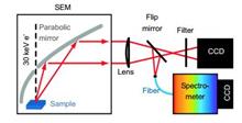
Scanning cathodoluminescence microscopy: applications in semiconductor and metallic nanostructures
Zhixin Liu, Meiling Jiang, Yanglin Hu, Feng Lin, Bo Shen, Xing Zhu, and Zheyu Fang
Cathodoluminescence (CL) as a radiative light produced by an electron beam exciting a luminescent material, has been widely used in imaging and spectroscopic detection of semiconductor, mineral and biological samples with an ultrahigh spatial resolution. Conventional CL spectroscopy shows an excellent performance in chCathodoluminescence (CL) as a radiative light produced by an electron beam exciting a luminescent material, has been widely used in imaging and spectroscopic detection of semiconductor, mineral and biological samples with an ultrahigh spatial resolution. Conventional CL spectroscopy shows an excellent performance in characterization of traditional material luminescence, such as spatial composition variations and fluorescent displays. With the development of nanotechnology, advances of modern microscopy enable CL technique to obtain deep valuable insight of the testing sample, and further extend its applications in the material science, especially for opto-electronic investigations at nanoscale. In this article, we review the study of CL microscopy applied in semiconductor nanostructures for the dislocation, carrier diffusion, band structure, doping level and exciton recombination. Then advantages of CL in revealing and manipulating surface plasmon resonances of metallic nanoantennas are discussed. Finally, the challenge of CL technology is summarized, and potential CL applications for the future opto-electronic study are proposed..
Opto-Electronic Advances
- Publication Date: Jun. 29, 2018
- Vol. 1, Issue 4, 180007-1 (2018)


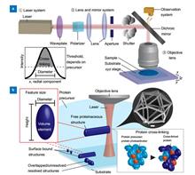
Fabrication of three-dimensional proteinaceous micro- and nano-structures by femtosecond laser cross-linking
Daniela Serien, and Koji Sugioka
Proteins are a class of biomaterials having a vast array of functions, including the catalysis of metabolic reactions, DNA replication, stimuli response and transportation of molecules. Recent progress in laser-based fabrication technologies has enabled the formation of three-dimensional (3D) proteinaceous micro- and nProteins are a class of biomaterials having a vast array of functions, including the catalysis of metabolic reactions, DNA replication, stimuli response and transportation of molecules. Recent progress in laser-based fabrication technologies has enabled the formation of three-dimensional (3D) proteinaceous micro- and nano-structures by femtosecond laser cross-linking, which has expanded the possible applications of proteins. This article reviews the current knowledge and recent advancements in the femtosecond laser cross-linking of proteins. An overview of previous studies related to fabrication using a variety of proteins and detailed discussions of the associated mechanisms are provided. In addition, advances and applications utilizing specific protein functions are introduced. This review thus provides a valuable summary of the 3D micro- and nano-fabrication of proteins for biological and medical applications..
Opto-Electronic Advances
- Publication Date: Jun. 07, 2018
- Vol. 1, Issue 4, 180008-1 (2018)