
Zhi Yan, Jingqi Hu, Zhexiang Xiao, Dale Xie, Qiang Cao, Zongsong Gan, Jingyu Zhang. Decoding the future: opportunities and challenges in next-generation optical data storage [Invited][J]. Chinese Optics Letters, 2023, 21(12): 120051
- Chinese Optics Letters
- Vol. 21, Issue 12, 120051 (2023)
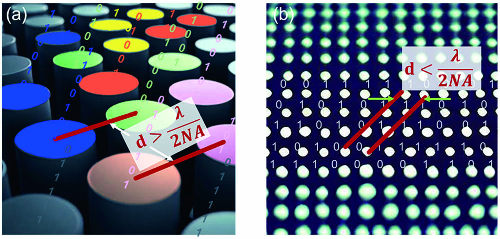
Fig. 1. (a) Multidimensional data storage: each data voxel is decoded into a sequence of binary data. (b) Superresolution data array: each data voxel is decoded into a single binary digit, but with higher spatial resolution.
![(a) Anisotropic light scattering generated within germanium-doped fused silica upon focusing femtosecond laser pulses of four polarization states[14]; (b) backscattering electron microscopy image of nanogratings[15]; (c) schematic of the nanogratings composed of periodic alignment of nanoplanes with different refractive index[16]; (d) erasing and rewriting capability of nanogratings[17].](/richHtml/col/2023/21/12/120051/img_002.jpg)
Fig. 2. (a) Anisotropic light scattering generated within germanium-doped fused silica upon focusing femtosecond laser pulses of four polarization states[14]; (b) backscattering electron microscopy image of nanogratings[15]; (c) schematic of the nanogratings composed of periodic alignment of nanoplanes with different refractive index[16]; (d) erasing and rewriting capability of nanogratings[17].
Fig. 3. (a), (b) Five-dimensional optical data storage with nanogratings in fused silica[30]; (c) five-dimensional optical storage writing setup with waveplate array[11]; (d) Arrhenius plot of the nanogratings decay rate[11]; (e) five-dimensional optical data storage via self-assembled nanogratings in fused silica. Maxwell and Newton are recorded in one image[31]. (f) Schematic illustration of the multidimensional shingled optical recording[33].
Fig. 4. (a) Bright field (left) and birefringence (right) microscopy images of anisotropic nanostructure produced in silica glass by a burst with pulse interval of 10 ps and with a single pulse for three different linear polarization directions, indicated by red arrows[35]; (b) schematic of formation mechanism of anisotropic nanostructure induced by spatiotemporal modulation and a birefringence microscopy image of an encoding array[36]; (c) birefringence and scanning electron microscopy images of anisotropic nanolamella-like structures via pulse energy modulation[37]; (d) birefringence and scanning electron microscopy images of single nanoslit structures[38]; (e) schematic diagram of the five-dimensional optical data storage writing setup based on Type X nanostructures[5]; (f) Project Silica and the GitHub Archive Program partnered to store and retrieve 114.8 GB of user data in a 75 mm × 75 mm × 2 mm piece of silica glass[12].
Fig. 5. (a), (b) Cis-isomer and trans-isomer conversion process of (a) azobenzene[41] and (b) diarylethene derivatives[42]; (c) photostable and thermostable anti-counterfeiting patterns on a photoresponsive conjugated polymer film[60]; (d) confocal microscopy image of bit patterns written into cis-1,2-dicyano-1,2-bis-(2,4,5-trimethyl-3-thienyl)ethene[71].
Fig. 6. (a) Schematic illustration of the gold nanorods reshaping due to photothermal effect under different light wavelengths and polarizations; (b) schematic diagram of five-dimensional optical data storage using gold nanorods[86]; (c) measurement of the 3D orientation of a single gold nanorod through two-photon fluorescence scanning images[87]; (d) distribution of two-photon absorption signals for an array of gold nanorods under excitation at 1070 nm wavelength with vertical polarization[90]; (e) schematic of the OAM-based six-dimensional optical data storage of quick response codes[93].
Fig. 7. (a) 3D optical data storage based on two-photon recording[103]; (b) encoding and decoding process of 3D optical data storage based on fluorescent silver cluster structures[104]; (c) erasing and recovery process of CsPbBr3 QD arrays under UV light[105]; (d) typical photoluminescence images of the multicolor patterns produced by femtosecond laser in glass[106].
Fig. 8. (a) 3D irreversible and reversible data storage using green-to-red photoconvertible fluorescent protein at excitation wavelength of 800 nm[123]; (b) audio recording and a BMP format image stored on the silk drive in binary format[127].
Fig. 9. (a) Schematic representation of the s-SNOM system: an infrared laser targets the AFM tip, with the resultant scattered signal captured by the detector. The system facilitates IR nanoimaging and measures the absorbance levels of UV–Silk30, UV–Silk90, UV–SilkHTP, and UV–LC across different exposure durations[130]. (b) Fluorescence microscopy beyond diffraction limits using asFP595. In the linearly deconvolved data, the peaks separated by 100-nm demonstrate a depth of 35%[131].
Fig. 10. (a) The writing beam triggers the reduction of GO via RET by transmitting high-energy quanta from UCNPs. Conversely, the inhibition beam prevents GO reduction by suppressing the generation of high-energy quanta in UCNPs. (b) Experimental arrangement for a dual-beam superresolution setup, facilitating the inscription of subdiffractional patterns on the nanocomposite[132].
Fig. 12. (a) Rewritable data storage depiction. Sequential writing and reading of 25 Grimm’s fairy tales (in ASCII code; 1.9 Mbits) on a 17 µm × 17 µm region of a PAA layer embedded with rsEGFP. Data bits are represented as spots (with selected frames displayed). The blue line sets the threshold to distinguish read spots as “0s” or “1s”[135]. (b) Demonstration of 3D parallelized recording through a volumetric superresolved multifocal array. SEM visuals display three layers of bit arrays documented by the superresolved multifocal array, maintaining a consistent bit size of 80 nm and a bit separation of 200 nm[136].
Fig. 13. Schematic illustration of key obstacles hindering the real-world applications of next-generation optical data storage.
Fig. 14. Schematic illustration of printed images with varying RERs. The corresponding error rate for each image is labeled to emphasize the impact of error rate on image quality.
Fig. 15. (a) The Code of Hammurabi; (b) doodles on a sandy beach.

Set citation alerts for the article
Please enter your email address
© Copyright 2018-2021 | Chinese Laser Press. All Rights Reserved 沪ICP备15018463号-20