Abstract
The ongoing quest for higher data storage density has led to a plethora of innovations in the field of optical data storage. This review paper provides a comprehensive overview of recent advancements in next-generation optical data storage, offering insights into various technological roadmaps. We pay particular attention to multidimensional and superresolution approaches, each of which uniquely addresses the challenge of dense storage. The multidimensional approach exploits multiple parameters of light, allowing for the storage of multiple bits of information within a single voxel while still adhering to diffraction limitation. Alternatively, superresolution approaches leverage the photoexcitation and photoinhibition properties of materials to create diffraction-unlimited data voxels. We conclude by summarizing the immense opportunities these approaches present, while also outlining the formidable challenges they face in the transition to industrial applications.
1. Introduction
In today’s digital age, we are witnessing an unprecedented surge in data generation. Factors such as the Internet of Things, big data analytics, artificial intelligence, and the increasing digitization of industries are contributing to an exponential growth in global data volume[1]. This has consequently led to heightened demands for efficient and reliable data storage solutions. While data are generated at rapid speeds, it is important to note that 80% of these data gradually transition to “cold” status as they age, moving from active usage to long-term archival needs[2]. Traditional storage methods like hard disk drives (HDDs) and magnetic tapes have served us well in the past but are now encountering serious limitations. These limitations are particularly evident in their lifespan of three to five years and capacity for storing cold data, making them less suitable as long-term archival solutions[3].
Optical data storage, distinguished by its offline storage capability and high-capacity attributes, has garnered considerable attention as a promising avenue for archiving cold data[3]. The emergence of advanced optical data storage technologies presents substantial opportunities, yet also poses significant challenges that research groups, startups, and large corporations around the globe are keen to address.
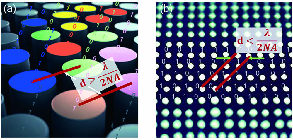
In this review, we undertake a comprehensive examination of recent advancements in the field of optical data storage technologies. Our analysis predominantly concentrates on two emerging paradigms that have the potential to revolutionize the domain. The first entails multidimensional data storage schemes, where multiple bits of information are encoded within a single data voxel, albeit constrained by diffraction limitation [Fig. 1(a)]. The second is superresolution optical data storage, where each voxel, transcending the bounds of the diffraction limits of light, contains a single bit of information [Fig. 1(b)]. Both roadmaps present compelling opportunities and challenges, and are subjects of increasing academic and industrial interest. This review aims to elucidate the underlying principles, technological advancements, and practical limitations of these approaches, thereby providing a cohesive understanding of the current landscape and future prospects of optical data storage.
Sign up for Chinese Optics Letters TOC. Get the latest issue of Chinese Optics Letters delivered right to you!Sign up now

Figure 1.(a) Multidimensional data storage: each data voxel is decoded into a sequence of binary data. (b) Superresolution data array: each data voxel is decoded into a single binary digit, but with higher spatial resolution.
2. Multidimensional Optical Data Storage
Conventional optical data storage techniques, such as DVDs and Blu-ray discs, are typically classified as two-dimensional (2D) optical data storage systems. In these systems, data voxels are confined to a prefabricated recording medium arranged in a 2D space. Consequently, the storage capacity of such media is generally limited, often capping at gigabyte-scale. While state-of-the-art Blu-ray technology has introduced multiple recording layers to augment capacity, these systems remain within the realm of multilayer data storage. The capacity is fundamentally constrained by the number of predefined layers, a figure that cannot be increased without limit.
Three-dimensional (3D) optical data storage, in contrast, takes full advantage of the bulk volume of isotropic materials. The salient difference between 3D and 2D optical storage lies in the spatial distribution of data voxels. In 3D systems, data voxels can be arbitrarily induced anywhere within the bulk material. Conversely, in 2D systems, voxels must be confined to predefined recording layers. With 3D data storage, data storing across hundreds of layers is not only possible but has also been experimentally demonstrated[4,5].
The advent of multidimensional data storage can be traced back to seminal work in 1989, which showed that data voxels could be formed through two-photon absorption in volume polymers[6]. Subsequent research by various teams has expanded on this pioneering discovery, exploring the potential for 3D optical data storage in a range of materials through two-photon or multiphoton absorption techniques[7,8]. However, these endeavors primarily stayed within the confines of the three spatial dimensions in isotropic media, and as such, the capacities remained constrained.
To transcend this limitation and further advance the field of multidimensional optical data storage, researchers have begun exploiting additional dimensions beyond the conventional three spatial ones. These involve intricate light–matter interactions, which have led to the development of several novel approaches. For the purposes of this review, these methodologies can be broadly categorized into three distinct roadmaps: birefringence-based methods, plasmon resonance-based techniques, and fluorescence-based approaches.
2.1. Optical data storage based on birefringence properties
Birefringence describes a phenomenon in which a single incident light ray results in two refracted rays. For anisotropic modification in isotropic bulk materials, this manifests as varying refractive indices based on light polarization. Controllable birefringence in these nanostructures facilitates four- or five-dimensional optical data storage, utilizing the slow-axis orientation and retardance dimension.
2.1.1. Nanogratings in glass for multidimensional optical storage
Silica glass is a highly durable and robust medium compared to the storage media used in current commercial data storage solutions. With its exceptional physical and chemical properties, silica glass is resilient against various adversities such as high temperatures, elevated pressures, microwaves, electromagnetic interference, and other environmental stressors. The wide bandgap of silica glass and its high transparency in the visible and infrared wavelength ranges allow a femtosecond laser to perform 3D printing of nanostructures inside the material via multiphoton ionization[9,10]. Owing to its outstanding mechanical and optical attributes, silica glass emerges as a trusted medium for upcoming optical data storage innovations[7,11,12].
Nanogratings in silica glass, characterized by their birefringence properties, emerge as one of the most promising solutions for next-generation multidimensional optical data storage[11,13]. These nanogratings incorporate not only a 3D spatial distribution but also two supplementary dimensions: retardance and slow-axis orientation. Together, they facilitate high-density, five-dimensional data storage.
The discovery of nanogratings can be traced back to 1999, when Kazansky et al. observed anisotropic light scattering in germanium-doped glass using femtosecond laser irradiation [Fig. 2(a)][14]. In the same year, Sudrie et al. conducted a similar observation in fused silica glass[18]. In 2003, Shimotsuma et al. identified the periodic polarized-dependent nanostructures in fused silica glass using backscattering electron microscopy, and referred to them as nanogratings [Fig. 2(b)][15]. Subsequently, research on the mechanisms[16,19–23] and applications[24–29] of nanogratings has been ongoing. Nanogratings orient perpendicular to the laser polarization direction, showcasing a birefringence characteristic similar to uniaxial crystals. This behavior arises from the periodic alignment of nanoplanes with a different refractive index [Fig. 2(c)][19]. This birefringence characteristic makes nanogratings suitable for multidimensional optical data storage [Figs. 3(a)–3(e)][11,30,31]. Moreover, femtosecond laser pulses can erase and rewrite this nanostructure [Fig. 2(d)][17,32], allowing for multiple repeated data recording[24,33]. Zhang et al. improved the data recording speed by configuring an array of wave plates in the writing setup [Fig. 3(c)] and verified the seemingly unlimited storage lifetime of the nanogratings [Fig. 3(d)][11]. Recently, the formation mechanism of nanogratings was comprehensively explained and a multidimensional shingled optical recording approach was demonstrated based on this mechanism [Fig. 3(f)][33,34]. Consequently, nanogratings stand out as a pivotal candidate for next-generation ultrahigh-density optical storage structures. However, in their application to multidimensional optical data storage, nanogratings face challenges chiefly concerning recording speed and pronounced scattering from multilayered recording structures.
Figure 2.(a) Anisotropic light scattering generated within germanium-doped fused silica upon focusing femtosecond laser pulses of four polarization states[14]; (b) backscattering electron microscopy image of nanogratings[15]; (c) schematic of the nanogratings composed of periodic alignment of nanoplanes with different refractive index[16]; (d) erasing and rewriting capability of nanogratings[17].
Figure 3.(a), (b) Five-dimensional optical data storage with nanogratings in fused silica[30]; (c) five-dimensional optical storage writing setup with waveplate array[11]; (d) Arrhenius plot of the nanogratings decay rate[11]; (e) five-dimensional optical data storage via self-assembled nanogratings in fused silica. Maxwell and Newton are recorded in one image[31]. (f) Schematic illustration of the multidimensional shingled optical recording[33].
2.1.2. Other anisotropic nanostructures in glass for multidimensional optical storage
To address the challenges posed by nanogratings in silica glass, researchers are making efforts to explore alternative solutions. Various anisotropic nanostructures have been induced in fused silica glass, leading to significant advancements in multidimensional optical data storage. High-speed induction of anisotropic structures can be achieved using temporal modulation [Fig. 4(a)][35] or spatiotemporal modulation [Fig. 4(b)][36], making the multidimensional data recording speed entirely dependent on the laser repetition rate. The storage density of nanogratings as a recording structure is constrained by the relatively large spatial occupancy from the periodic arrangement of nanoplanes. In contrast, the width of a nanolamella-like structure [Fig. 4(c)][37] or a single nanoslit [Fig. 4(d)][38] is only a few tens of nanometers. These compact anisotropic structures, being smaller than the diffraction limitation, can significantly boost storage density. And the type X nanostructure, made up of anisotropic nanopores and recognized for its ultralow-light loss[39], enables nearly error-free reading of multilayered data [Fig. 4(e)][5]. Notably, elliptical polarization further enhances its recording efficiency[40].
Figure 4.(a) Bright field (left) and birefringence (right) microscopy images of anisotropic nanostructure produced in silica glass by a burst with pulse interval of 10 ps and with a single pulse for three different linear polarization directions, indicated by red arrows[35]; (b) schematic of formation mechanism of anisotropic nanostructure induced by spatiotemporal modulation and a birefringence microscopy image of an encoding array[36]; (c) birefringence and scanning electron microscopy images of anisotropic nanolamella-like structures via pulse energy modulation[37]; (d) birefringence and scanning electron microscopy images of single nanoslit structures[38]; (e) schematic diagram of the five-dimensional optical data storage writing setup based on Type X nanostructures[5]; (f) Project Silica and the GitHub Archive Program partnered to store and retrieve 114.8 GB of user data in a 75 mm × 75 mm × 2 mm piece of silica glass[12].
These anisotropic structures promise high data density[33,37] and precise readout[5]. Furthermore, compared to other multidimensional storage methods, anisotropic nanostructures in silica glass stand out as one of the most commercially feasible solutions. The Project Silica initiative has successfully accomplished the storage and retrieval of 114.8 GB of user data in its entirety [Fig. 4(f)][12]. However, optical devices used for multidimensional data readout tend to be intricate and cumbersome, not aligning with commercial application requirements. This calls for deeper research into novel storage media, recording and readout mechanisms, swift data extraction algorithms, and notably, miniaturization of storage systems.
2.1.3. Laser-induced birefringence in organic materials for multidimensional optical storage
Unlike the birefringence property of anisotropic nanostructures, laser-induced birefringence in organic materials arises from molecular-level anisotropy. Such organic materials enable repetitive adjustments of birefringence through laser irradiation and find application in rewritable multidimensional optical data storage applications[41–45]. Two primary types of organic materials, azo dyes [Fig. 5(a)] and diarylethene derivatives [Fig. 5(b)], are capable of inducing birefringence and are employed in multidimensional optical storage applications.
Figure 5.(a), (b) Cis-isomer and trans-isomer conversion process of (a) azobenzene[41] and (b) diarylethene derivatives[42]; (c) photostable and thermostable anti-counterfeiting patterns on a photoresponsive conjugated polymer film[60]; (d) confocal microscopy image of bit patterns written into cis-1,2-dicyano-1,2-bis-(2,4,5-trimethyl-3-thienyl)ethene[71].
Azo molecules typically assume a stable trans configuration under standard conditions (room temperature, anechoic chamber)[46]. However, when exposed to polarized light, they can transition between cis and trans isomers [Fig. 5(a)][41,47,48], resulting in the emergence of optical anisotropy. This optical anisotropy primarily in azo materials arises from two different mechanisms: angular hole burning[49] and angular redistribution of the molecule[50]. Due to their excellent photoinduced anisotropic properties, azo materials exhibit vast potential applications in the field of optical storage. A common method involved directly doping azo materials into organic carriers like polyvinyl alcohol (PVA)[51,52] or polymethyl methacrylate (PMMA)[53,54]. In addition, the photoinduced anisotropy of azo molecules exhibits higher resolution for image storage when irradiated with coherent light, as opposed to incoherent light[55]. Li et al. achieved erasable, polarization-encoded multilayer data storage on polymer films doped with the azo dye 2,5-dimethyl-4-(p-nitrophenylazo)anisole (DMNPAA)[56]. However, these materials exhibit thermal isomerization characteristics, resulting in relatively weak thermal stability. This not only necessitates more stringent storage conditions but also leads to shorter storage lifespans. The thermal stability of azobenzene materials can be enhanced by incorporating azobenzene molecules into polymers as main-chain and side-chain polymers through chemical bonding[57–59]. For instance, a photoresponsive conjugated polymer, which contains alternating azobenzene and fluorene units, exhibits high thermal stability at 370°C [Fig. 5(c)][60]. Furthermore, the photoinduced anisotropy of liquid-crystal materials containing azobenzene moieties demonstrates reverse relaxation characteristics, enhancing their ability for long-term high-density data storage[61–67]. However, thermal effects during photoisomerization cycles still persist[68,69], compromising the photoinduced birefringence. Exploring methods to mitigate these thermal effects will be a crucial research direction for the application of azo materials in optical storage.
The mechanism of photoinduced birefringence in diarylethene derivatives is similar to that of azobenzene molecules, but it does not undergo thermal isomerization[42–44,70]. Therefore, it exhibits excellent thermal stability and fatigue resistance. Its high quantum yield and the ability for multiple write-erase cycles[71] make it highly valuable in the field of optical storage [Fig. 5(d)][72] and holographic storage[73,74]. Although most diarylethene derivatives exhibit good thermal stability and fatigue resistance, the process of writing and erasing requires different wavelengths of light [ultraviolet (UV) and visible light], which adds complexity to optical data storage systems.
2.2. Multidimensional optical storage based on plasmon resonance
Different from the aforementioned birefringence properties, plasmon resonance expands dimension multiplexing by triggering distinct responses from nanoparticles of varied shapes and sizes to specific wavelengths and polarizations. Gold nanorods, precisely due to this plasmon resonance property[75,76], emerge as another promising candidate medium for multidimensional optical data storage[77]. These nanostructures exhibit a narrow longitudinal surface plasmon resonance () linewidth in the near-infrared wavelength range[78,79]. The shape of the nanorods dictates the plasmon resonance wavelength of these nanostructures[78]. This shape-dependent property is crucial for multidimensional optical storage using spectral encoding[80]. Furthermore, photothermal effects from femtosecond laser pulse irradiation can reshape gold nanorods[81-83]. Their dipolar optical response grants them wavelength and polarization selectivity for femtosecond laser-resonant photothermal effect [Fig. 6(a)][84,85]. Leveraging these characteristics, in 2009, Zijlstra et al. were the pioneers in using gold nanorods for five-dimensional optical data recording [Fig. 6(b)][86]. Subsequently, research on the use of gold nanorods for multidimensional data storage has subsequently gained momentum.
Figure 6.(a) Schematic illustration of the gold nanorods reshaping due to photothermal effect under different light wavelengths and polarizations; (b) schematic diagram of five-dimensional optical data storage using gold nanorods[86]; (c) measurement of the 3D orientation of a single gold nanorod through two-photon fluorescence scanning images[87]; (d) distribution of two-photon absorption signals for an array of gold nanorods under excitation at 1070 nm wavelength with vertical polarization[90]; (e) schematic of the OAM-based six-dimensional optical data storage of quick response codes[93].
Li et al. expanded the polarization response of gold nanorods to three dimensions by employing a vector beam with 3D polarization orientations [Fig. 6(c)][87]. Furthermore, Zhang et al. achieved an extended storage lifetime of gold nanorods for several centuries by doping them into a hybrid glass with a higher Young’s modulus[88]. Through plasmonic coupling, gold nanorods can create random hot spots [Fig. 6(d)][89–91]. These hot spots drastically reduce the needed recording energy—by almost 2 orders of magnitude—and boost multiplexing capacity, paving the way for ultrahigh-density optical data storage. Xian et al. capitalized on the response of gold nanorods to cylindrical vector beams, using the order of the cylindrical vector beams as another dimension for data storage[92]. Xu et al. highlighted that tightly focused linearly polarized orbital angular momentum (OAM) beams with different topological charges result in distinct polarization ellipses at the same position within the focal spot, facilitating the emergence of nanoscale synthetic helical dichroism[93]. This brings forth OAM as a sixth dimension, transcending five-dimensional optical data storage [Fig. 6(e)].
Multidimensional optical data storage solutions leveraging gold nanorods present significant benefits in storage dimensions. Nonetheless, challenges persist, such as intricate material fabrication, compromised stability, and a limited number of gold nanorods in the focal volume and signal interference, limiting their commercial viability. For improved applicability, there is a pressing need to streamline equipment and material procedures and bolster the stability of the recording structures and substrates. Continued research focus into these directions is imperative.
2.3. Multidimensional optical storage based on fluorescence
2.3.1. Two-photon absorption for multidimensional optical storage
By harnessing the two-photon absorption characteristics of certain polymer materials[94,95], it is possible to achieve two-photon voxel writing, reading, and erasing. This is due to the fact that the ground-state electrons in these polymer materials can simultaneously absorb two photons, resulting in their transition to an excited state[96,97]. This enables the realization of ultrahigh-density 3D optical data storage technology[6,98–100], whose storage capacity surpassing that of DVD and Blu-ray by a factor of 100[99]. Furthermore, compared to single-photon processing, this technique exhibits lower cross talk, resulting in a higher signal-to-noise ratio during the readout process[101]. Subsequently, Cumpston et al. successfully accomplished two-photon polymerization for 3D optical data storage using a class of -conjugated compounds that exhibit large two-photon absorption cross sections[102]. Walker et al. achieved successful two-photon recording of multilayer fluorescence voxels using alternative materials with their disc consisting of 200 layers, each containing 5 GB of data, while achieving a writing speed of up to 25 Mbit/s [Fig. 7(a)][103]. In the future, enhancing the writing speed, durability, and overall efficiency is crucial for the multidimensional optical storage techniques based on two-photon absorption. The exploration of integrating supplementary optical attributes, such as polarization[86], holds the potential for realizing advanced higher-dimensional optical storage solutions[3].
Figure 7.(a) 3D optical data storage based on two-photon recording[103]; (b) encoding and decoding process of 3D optical data storage based on fluorescent silver cluster structures[104]; (c) erasing and recovery process of CsPbBr3 QD arrays under UV light[105]; (d) typical photoluminescence images of the multicolor patterns produced by femtosecond laser in glass[106].
2.3.2. Photoluminescence in glass for multidimensional optical storage
Glass possesses qualities such as excellent light transmission, strong chemical stability, and favorable mechanical properties. Femtosecond lasers have the capability to induce defects with photoluminescent properties[107,108] inside silica glass, enabling 3D optical data storage. However, the intensity of this fluorescence is low, and the thermal stability is relatively poor. Subsequent researchers explored methods such as rare-earth ion doping[109] or quantum dot (QD)[110] induction to enhance fluorescence intensity and stability.
The crystalline phases in glass ceramics provide distinct sites for rare-earth ions, which helps enhance the intensity and lifetime of fluorescence. Additionally, femtosecond lasers can induce changes in the valence states of rare-earth ions, promoting their applications in 3D optical storage[111]. By manipulating the valence state changes of samarium ions using femtosecond lasers, it has been demonstrated that a storage density of can be achieved[112,113]. Furthermore, silver-doped glass materials can be modified by femtosecond lasers to possess fluorescent silver cluster structures, making them suitable for 3D[104,114] and even higher-dimensional optical data storage [Fig. 7(b)][115].
QDs are a novel type of optical material with tunable photoluminescence, high quantum efficiency, broad absorption range, and resistance to photobleaching. A femtosecond laser combined with other methods such as thermal treatment[105] and moisture field modulation[110] can induce, erase, and rewrite perovskite QDs in perovskite glass [Fig. 7(c)]. This makes laser-induced in-glass perovskite QDs a promising avenue for multidimensional optical storage applications[105,110,116]. The introduction of polarized structures can also achieve higher-capacity data encryption[116]. Recently, it has been demonstrated that the irradiation time of femtosecond lasers can be used to adjust the elemental ratios, allowing for wavelength-tunable luminescence of perovskite QDs in glass [Fig. 7(d)][106].
2.3.3. Fluorescent protein for multidimensional optical storage
As a representative biological material, protein has various and complex structures, endowing it with excellent electrical, optical, mechanical, chemical, and electromagnetic properties[117–121] that are suitable for optical data storage. The photochromic property of bacteriorhodopsin (bR) imparts its ability for wavelength-multiplexed optical data storage[122]. Additionally, when combined with its 2D crystalline arrangement, optical data rewriting becomes achievable [Fig. 8(a)][123]. Moreover, fluorescent proteins with photoactivation and photoconversion capabilities exhibit rapid and reversible photon blinking, offering them an advantageous application in the field of optical reversible data storage[124–126]. In addition to relying solely on protein fluorescence, optical data storage can also be achieved by manipulating the protein morphology. Advanced nanopatterning techniques, such as tip-enhanced nano-optics, can induce surface morphology changes in silk fibroin [Fig. 8(b)][127]. This writing approach demonstrates significant storage capacity along with compatibility with biological interfaces.
Figure 8.(a) 3D irreversible and reversible data storage using green-to-red photoconvertible fluorescent protein at excitation wavelength of 800 nm[123]; (b) audio recording and a BMP format image stored on the silk drive in binary format[127].
3. Superresolution Optical Storage
With the rapid development of big data and electronic information technology, the demand for data storage capacity and readout speed has been consistently increasing. Information storage methods primarily based on magnetic storage technology suffer from shortcomings such as short storage times and high energy consumption. In comparison to magnetic storage, optical storage technology offers advantages like low energy consumption and high data security[128]. However, the capacity of optical storage is greatly constrained by the optical diffraction limit. Overcoming the optical diffraction limit to achieve superresolution storage is the key to enhancing data storage capacity[129].The optical diffraction limit formula reveals that resolution mainly depends on the wavelength of incident light and the numerical aperture (NA). Therefore, methods to increase optical storage capacity mainly focus on shortening the wavelength of incident light and using higher NA objectives. Nevertheless, the incident wavelength has already reached the extreme UV range, and the NA of objective lenses is also limited by a technical bottleneck. Furthermore, using laser light sources with shorter wavelengths will result in a more intricate optical system, requiring costly optical components, thus increasing the cost of optical storage. Therefore, in order to meet the needs of high-efficiency and high-density optical storage, it is particularly important to study and develop superresolution optical storage technology beyond the optical diffraction limit.
3.1. Superresolution optical storage based on proteins
UV photolithographic patterning of protein-based microstructures has demonstrated the use of proteins as resist materials. The fatal weakness of existing protein-based biophotoresists is the unavoidable broad molecular weight distribution in the protein extraction/regeneration process, which hinders their practical application in the optical data storage industry, and repeatability is of paramount importance [Fig. 9(a)][130]. Tao et al. used silk fibroin light chains as a resist, and high-resolution patterning of biological microstructures was obtained[130]. Wafer-level high-resolution patterned materials with biological microstructures have shown unprecedented performance. This protein photoresist has higher image resolution, better etching resistance, and inherent biocompatibility, which provides new opportunities for the fabrication of large-scale biocompatible functional microstructures. Hofmann et al. demonstrated a reversible photoswitching protein between a fluorescence-activated state and a nonactivated state (RESOLFT) type of concept to resolve 50–100 nm in the focal plane [Fig. 9(b)][131].
Figure 9.(a) Schematic representation of the s-SNOM system: an infrared laser targets the AFM tip, with the resultant scattered signal captured by the detector. The system facilitates IR nanoimaging and measures the absorbance levels of UV–Silk30, UV–Silk90, UV–SilkHTP, and UV–LC across different exposure durations[130]. (b) Fluorescence microscopy beyond diffraction limits using asFP595. In the linearly deconvolved data, the peaks separated by 100-nm demonstrate a depth of 35%[131].
3.2. Superresolution optical storage based on upconversion nanoparticles
Lanthanide-doped upconverting nanoparticles (UCNPs) can optically convert low-energy near-infrared beams into high-energy UV or visible photons, facilitating photoactivation in optical data storage.
Lamon et al. demonstrated nanoscale optical writing using UCNPs and graphene oxide (GO) as substrates [Fig. 10][132]. The resonance energy transfer (RET) of high-energy quanta from UCNPs induces a localized chemical reduction in GO flakes, with two-beam superresolution irradiation, achieving optical writing with a lateral feature size of (1/20 of the wavelength) at a rejection intensity of [132].
Figure 10.(a) The writing beam triggers the reduction of GO via RET by transmitting high-energy quanta from UCNPs. Conversely, the inhibition beam prevents GO reduction by suppressing the generation of high-energy quanta in UCNPs. (b) Experimental arrangement for a dual-beam superresolution setup, facilitating the inscription of subdiffractional patterns on the nanocomposite[132].
3.3. Superresolution optical storage based on stimulated emission depletion
In 1994, Hell introduced stimulated emission depletion (STED) fluorescence microscopy while researching far-field microscopy imaging[133]. As shown in Fig. 11(a), the method utilizes two beams of light. The first beam excites the molecules from the ground state L0 to the higher vibrational state L1. The electrons in the higher vibrational state will transition to the lowest vibrational state L2 through vibrational relaxation. The second beam of loss light will quench the excitation of the fluorescent molecules in the excited state, thereby transitioning to the higher vibrational state L3 of the ground state and then returning to the lowest vibrational state L0 of the ground state through vibrational relaxation. This method uniquely uses two beams of light to control the excitation of the material. The most striking feature is that under the excitation of one beam, the other beam spatially modulates the fluorescence signal in the excitation region by induced stimulated emission losses. This breakthrough successfully surpassed the limitation of optical diffraction [Fig. 11(b)][134].
Figure 11.(a) Schematic diagram of STED[133]; (b) schematic diagram of the STED device[134].
Based on the concept of STED, introducing a dual-beam optical system in optical data storage devices could reduce information recording to the nanoscale level, thereby realizing the optical storage requirements of ultrahigh capacity and ultrafast data. In 2011, Grotjohann et al. utilized a novel fluorescent protein (called reversibly switchable enhanced green fluorescent protein, rsEGFP)[135]. Combined with the double-beam superresolution technology [Fig. 12(a)], they converted the text of 25 Grimm’s fairy tales into 7-bit binary ASCII format and inscribed 270,000 letters within a region across 6596 frames, with every frame accommodating 41 letters. Each individual bit spanned a diameter of 500 nm[135]. In 2015, Li et al. parallelized recording of binary bits with a feature size below the diffraction limit [Fig. 12(b)][136]. By using a femtosecond pulse laser beam with a wavelength of 800 nm as the excitation beam and a continuous-wave laser beam with a wavelength of 532 nm as the inhibition beam, a recording spot of 200 nm is realized on the optical disk and the capacity of a single optical disk achieves 30 TB[136].
Figure 12.(a) Rewritable data storage depiction. Sequential writing and reading of 25 Grimm’s fairy tales (in ASCII code; 1.9 Mbits) on a 17 µm × 17 µm region of a PAA layer embedded with rsEGFP. Data bits are represented as spots (with selected frames displayed). The blue line sets the threshold to distinguish read spots as “0s” or “1s”[135]. (b) Demonstration of 3D parallelized recording through a volumetric superresolved multifocal array. SEM visuals display three layers of bit arrays documented by the superresolved multifocal array, maintaining a consistent bit size of 80 nm and a bit separation of 200 nm[136].
Figure 13.Schematic illustration of key obstacles hindering the real-world applications of next-generation optical data storage.
With the continuous development of various superresolution technologies, the optical storage technology based on superresolution is also consistently improving and maturing. The theoretical storage density of optical data storage technology continues to expand, which enables it to overcome the shortcomings of other data storage methods, such as high energy consumption and low lifetime of magnetic storage technology. It has a wide application prospect in big data storage technology.
4. Discussions
While these novel approaches to multidimensional and superresolution optical data storage present significant advantages in terms of data capacity, a variety of challenges must be addressed before these technologies can be successfully implemented in industrial applications. Major obstacles include factors such as the time required to induce data voxels, raw error rate (RER), storage lifetime, system development, algorithm evolution, cost, and industrial viability.
4.1. Time required to induce data
Data storage is intrinsically a process where a signal induces a change in the storage medium, whether that medium responds optically, electrically, or magnetically. This interaction time is determined by the specific physical or chemical processes occurring in the recording medium, and must be minimized for high-speed data storage. And for optical data storage, the fundamental constraint is the time required for light–material interaction.
To put this into perspective, consider that if a writing speed of 10 MB/s is required and each voxel represents a single bit of information, approximately 80 million voxels would need to be modified per second. Neglecting the time it takes to move the writing mechanism from one voxel to another, each voxel would have only 12.5 ns for modification. In reality, travel time between voxels cannot be ignored and further constrains the time available for each voxel modification. Traditional storage techniques such as HDDs, DVDs, and Blu-ray discs operate with signal–material interaction times in the subnanosecond range. While much of the existing research on next-generation optical data storage has focused on advancements in technology, the signal–material interaction time often remains overlooked[11,86,106,127]. This time constraint can serve as a valuable benchmark for evaluating the feasibility of new techniques for real-world applications.
For instance, the utilization of gold nanorods in optical data storage typically requires a laser duration on the millisecond time scale to induce a single voxel[88]. Consequently, in a single-beam arrangement, a maximum of only a few tens or hundreds of voxels can be formed each second. Similarly, STED-based techniques may offer the capability to surpass the diffraction limitation, but they come with their own set of challenges. The required stimulation and inhibition processes necessitate a complex optical setup and specific laser irradiation sequences. To illustrate, superresolution approaches employing rsEGFP mandate a four-step writing process[135]. Even under ideal conditions, assuming perfect synchronization and negligible heat accumulation, the total light irradiation time exceeds 20 ms. This severely restricts the number of voxels that can be induced within a given period.
Several approaches are actively addressing the challenges posed by light–material interaction time. For instance, in the realm of five-dimensional optical data storage based on birefringence nanostructures in glass, conventional methods often necessitate tens of pulses to induce a single nanostructure[11,38]. This requirement poses a significant bottleneck for data writing speed. However, recent advancements have shown promise in circumventing this limitation. Researchers have discovered that spatiotemporal manipulation of picosecond beams can effectively induce birefringence nanostructures[36]. This technological leap allows for on-the-fly recording capabilities comparable to those of traditional Blu-ray storage systems. In another noteworthy development, the implementation of a pulse sequence scheme has reduced the number of required pulses to merely five[37,137]. This innovation has the potential to elevate data writing speeds to megabytes per second. Similar innovative solutions have also been demonstrated in other material systems, including glass-based[138] and polymer-based[139] optical data storage.
In summary, these emerging strategies demonstrate the industry’s commitment to resolving the challenges associated with light–material interaction time. Such advances mark crucial steps in transitioning these next-generation technologies from the research stage to commercial implementation.
4.2. Raw error rate
One of the often-overlooked parameters in the research of optical data storage technologies is the RER, a critical factor for industrial applications. The prevailing trend in academic studies is to showcase the technology’s ability to record arbitrary data by imprinting a voxel array with a scene, portrait, or binary code[140–142]. While such demonstrations offer an intuitive impression of the technology’s capability, they can be misleading for several reasons.
Primarily, these demonstrations imply that if one can successfully print an image, the same technology should be able to record real data. This implication is flawed, as human perception has a high tolerance to errors in image quality. For instance, we generated a series of images programmatically that showed better contrast and resolution than many state-of-the-art demonstrations. However, only one of these images achieved an RER of 1% [Fig. 14(a)]. In contrast, the image with the poorest performance had an RER of 40%, which is quite significant yet still produced a visually acceptable image to the human eye [Fig. 14(d)]. It is worth noting that the theoretical maximum error rate for a binary system is 50%. Therefore, relying solely on visual demonstrations for proof of concept might not capture the full scope of challenges in reducing the RER to a level acceptable for industrial applications.
Figure 14.Schematic illustration of printed images with varying RERs. The corresponding error rate for each image is labeled to emphasize the impact of error rate on image quality.
In the context of real-world applications, it is crucial to understand that the operational environment can exacerbate the RER. The complexity of the optical paths and the recording medium introduces a variety of noise, thereby increasing the likelihood of random error behavior. Additionally, during the data retrieval process, factors such as dynamic servo and surface scratches on the disc contribute to data errors. These environmental and operational challenges underline the importance of developing robust read-write systems to ensure the efficacy of optical data storage systems.
4.3. Lifetime
In the realm of data storage, optical media generally possess a longer lifespan compared to their electronic and magnetic counterparts. However, the longevity of optical storage is contingent on both the recording principles employed and the materials used. A broadly accepted notion posits that the more effort invested in the recording process, the greater the data longevity. The magnitude of this effort is fundamentally determined by the recording medium. For example, the ancient Babylonians’ painstaking inscription has enabled the Code of Hammurabi to endure for nearly four millennia [Fig. 15(a)]. In contrast, casual doodles on a sandy beach are quickly erased by the ocean’s tides [Fig. 15(b)]. Despite both being forms of inscription, the differing media and levels of effort result in vastly disparate lifetimes.
Figure 15.(a) The Code of Hammurabi; (b) doodles on a sandy beach.
Recent studies have indicated that the Young’s modulus of the recording material is a key factor influencing data longevity[88]. Silica glass, a robust material with a high Young’s modulus, has proven to be particularly durable[19]. Various forms of laser-induced modifications in glass—known as Type I[143], Type II[11,30], Type III[7,144], and Type X[5]—have all demonstrated extremely long lifetimes, making them attractive options for optical data storage. However, this longevity comes at a cost. Materials with a high Young’s modulus require more intense laser beams or longer irradiation periods[88], both of which have practical limitations. The necessity for high-power or ultrafast lasers inflates system costs, while extended irradiation times compromise data writing speeds. Striking an optimal balance between data longevity and system practicality remains an open challenge. Advances in material science and laser processing techniques are anticipated to pave the way for photon-efficient laser writing in robust materials, mitigating some of the existing trade-offs.
4.4. System development
The journey from a laboratory breakthrough to a real-world application is not linear. For next-generation optical data storage to move beyond academic circles and become a staple in industry, the development of a complete write/read system is essential. Currently, many optical data storage systems, especially those involving advanced laser setups in laboratory, are bulky and complex. Miniaturization is paramount for a more seamless integration into industrial processes and for enhancing user experience. Leading the way in this regard is a multidimensional storage solution based on quartz glass, from Hitachi’s 3D silica storage solution[145] in the early days to Microsoft’s Project Silica[12,13] today. Although the commercialization of these solutions is still in its infancy, it does provide a clear direction for the next-generation optical data storage. Over time, after the high integration of femtosecond lasers, the advantages of silica storage solutions will become more obvious.
4.5. Algorithm evolution
Equally pivotal is the evolution of write/read algorithms. The vast amounts of data that next-generation optical data storage systems promise to handle necessitate advanced algorithms for efficient data retrieval and storage. Artificial intelligence can be a game-changer in this realm. Already, in recent optical data storage research works, artificial intelligence algorithms have demonstrated their prowess in enhancing data access speeds and reliability[13,146,147]. By leveraging pattern recognition and predictive analytics, artificial intelligence can optimize data retrieval paths, preemptively address errors, and streamline data storage, thus bridging the gap between theoretical storage capabilities and practical performance.
4.6. Cost and industrial viability
Despite the enticing prospects of high-density, rapid, and long-lasting storage capabilities, the elephant in the room remains the cost of implementation. Today, HDD and recording magnetic-based tapes are the dominant players when it comes to storing cold data in many industrial sectors. The reasons are simple: they are cost-effective and reliable. For optical data storage to become a strong contender in the data storage market, the costs must compete with, if not undercut, existing solutions. Magnetic tape-based storage is priced at approximately $7 per terabyte[148], whereas other optical and disk-driven alternatives are around $14 per terabyte[149]. If next-generation optical data storage cannot reach or approach this price point, its commercial uptake remains questionable, irrespective of its technical advantages. High densities, rapid write/read speed, and impressive lifetime are attractive selling points, but in the real world, the bottom line of cost often dictates eventual adoption. It is imperative for optical data storage researchers and developers to consider these practical aspects, diving deep into material science innovations, manufacturing optimizations, and bulk production possibilities to make optical data storage an economically viable alternative.
5. Conclusion
In conclusion, both multidimensional and superresolution optical data storage techniques exhibit substantial promise, particularly in terms of their data capacity, aligning well with the exponential surge in global data generation. However, several significant challenges remain unaddressed, including the time required for data voxel induction, RER, lifetime, system development, algorithm evolution, cost, and industrial viability. Encouragingly, there has been a palpable shift in the research community toward addressing these practical obstacles in an effort to transition these technologies from the experimental stage to industrial applicability. It is our aspiration that readers of this review will gain a comprehensive understanding of the state of the art, and perhaps more importantly, a sense of confidence in the future prospects of next-generation optical data storage. We earnestly hope that this insight will galvanize both researchers and industry companies to invest further resources into this burgeoning field, thereby accelerating the advent of truly scalable, efficient, and long-lasting optical data storage solutions.
References
[1] R. David, G. John, R. John. The digitization of the world from edge to core(2018).
[2] D. Reinsel, L. Wu, J. F. Gantz, J. Rydning. The China Datasphere: primed to be the largest datasphere by 2025(2019).
[3] M. Gu, X. Li, Y. Cao. Optical storage arrays: a perspective for future big data storage. Light-Sci. Appl., 3, e177(2014).
[4] E. Walker, P. M. Rentzepis. Two-photon technology: a new dimension. Nat. Photonics, 2, 406(2008).
[5] H. Wang, Y. Lei, L. Wang, M. Sakakura, Y. Yu, G. Shayeganrad, P. G. Kazansky. 100-layer error-free 5D optical data storage by ultrafast laser nanostructuring in glass. Laser Photonics Rev., 16, 2100563(2022).
[6] D. A. Parthenopoulos, P. M. Rentzepis. Three-dimensional optical storage memory. Science, 245, 843(1989).
[7] E. N. Glezer, M. Milosavljevic, L. Huang, R. J. Finlay, T. H. Her, J. P. Callan, E. Mazur. Three-dimensional optical storage inside transparent materials: errata. Opt. Lett., 22, 422(1997).
[8] Y. Kawata, H. Ueki, Y. Hashimoto, S. Kawata. Three-dimensional optical memory with a photorefractive crystal. Appl. Opt., 34, 4105(1995).
[9] S. Tzortzakis, L. Sudrie, M. Franco, B. Prade, A. Mysyrowicz, A. Couairon, L. Bergé. Self-guided propagation of ultrashort IR laser pulses in fused silica. Phys. Rev. Lett., 87, 213902(2001).
[10] A.-C. Tien, S. Backus, H. Kapteyn, M. Murnane, G. Mourou. Short-pulse laser damage in transparent materials as a function of pulse duration. Phys. Rev. Lett., 82, 3883(1999).
[11] J. Zhang, M. Gecevicius, M. Beresna, P. G. Kazansky. Seemingly unlimited lifetime data storage in nanostructured glass. Phys. Rev. Lett., 112, 033901(2014).
[12] P. Anderson, E. Aranas, R. Black, S. Bucciarelli, M. Caballero, P. Cameron, B. Canakci, A. Chatzieleftheriou, J. Clegg, D. Cletheroe, B. Cooper, T. Deegan, A. Donnelly, R. Drevinskas, C. Gkantsidis, A. Gomez Diaz, I. Haller, P. Heard, T. Ilieva, R. Joyce, S. Legtchenko, B. Magalhaes, A. Ogus, A. Rowstron, M. Sakakura, N. Schreiner, A. Smith, I. Stefanovici, D. Sweeney, P. Wainman, C. Whittaker, H. Williams, T. Winkler, S. Winzeck, L. Gemini, A. Narazaki, J. Kleinert. Multi-dimensional optical data writing techniques for cloud-scale archival storage. Proc. SPIE, 12408, 1240807(2023).
[13] P. Anderson, E. B. Aranas, Y. Assaf, R. Behrendt, R. Black, M. Caballero, P. Cameron, B. Canakci, T. D. Carvalho, A. Chatzieleftheriou, R. S. Clarke, J. Clegg, D. Cletheroe, B. Cooper, T. Deegan, A. Donnelly, R. Drevinskas, A. Gaunt, C. Gkantsidis, A. G. Diaz, I. Haller, F. Hong, T. Ilieva, S. Joshi, R. Joyce, M. Kunkel, D. Lara, S. Legtchenko, F. L. Liu, B. Magalhaes, A. Marzoev, M. Mcnett, J. Mohan, M. Myrah, T. Nguyen, S. Nowozin, A. Ogus, H. Overweg, A. Rowstron, M. Sah, M. Sakakura, P. Scholtz, N. Schreiner, O. Sella, A. Smith, I. Stefanovici, D. Sweeney, B. Thomsen, G. Verkes, P. Wainman, J. Westcott, L. Weston, C. Whittaker, P. W. Berenguer, H. Williams, T. Winkler, S. Winzeck. Project Silica: towards sustainable cloud archival storage in glass. Proceedings of the 29th Symposium on Operating Systems Principles(2023).
[14] P. G. Kazansky, H. Inouye, T. Mitsuyu, K. Miura, J. Qiu, K. Hirao. Anomalous anisotropic light scattering in Ge-doped silica glass. Phys. Rev. Lett., 82, 2199(1999).
[15] Y. Shimotsuma, P. G. Kazansky, J. Qiu, K. Hirao. Self-organized nanogratings in glass irradiated by ultrashort light pulses. Phys. Rev. Lett., 91, 247405(2003).
[16] V. R. Bhardwaj, E. Simova, P. P. Rajeev, C. Hnatovsky, R. S. Taylor, D. M. Rayner, P. B. Corkum. Optically produced arrays of planar nanostructures inside fused silica. Phys. Rev. Lett., 96, 057404(2006).
[17] R. S. Taylor, C. Hnatovsky, E. Simova, P. P. Rajeev, D. M. Rayner, P. B. Corkum. Femtosecond laser erasing and rewriting of self-organized planar nanocracks in fused silica glass. Opt. Lett., 32, 2888(2007).
[18] L. Sudrie, M. Franco, B. Prade, A. Mysyrowicz. Writing of permanent birefringent microlayers in bulk fused silica with femtosecond laser pulses. Opt. Commun., 171, 279(1999).
[19] E. Bricchi, P. G. Kazansky. Extraordinary stability of anisotropic femtosecond direct-written structures embedded in silica glass. Appl. Phys. Lett., 88, 111119(2006).
[20] Y. Bellouard, A. Champion, B. McMillen, S. Mukherjee, R. R. Thomson, C. Pépin, P. Gillet, Y. Cheng. Stress-state manipulation in fused silica via femtosecond laser irradiation. Optica, 3, 1285(2016).
[21] B. Poumellec, M. Lancry, R. Desmarchelier, E. Herve, B. Bourguignon. Parity violation in chiral structure creation under femtosecond laser irradiation in silica glass?. Light-Sci. Appl., 5, e16178(2016).
[22] A. Rudenko, H. Ma, V. P. Veiko, J.-P. Colombier, T. E. Itina. On the role of nanopore formation and evolution in multi-pulse laser nanostructuring of glasses. Appl. Phys. A, 124, 63(2017).
[23] A. Rudenko, J. P. Colombier, T. E. Itina. Nanopore-mediated ultrashort laser-induced formation and erasure of volume nanogratings in glass. Phys. Chem. Chem. Phys., 20, 5887(2018).
[24] R. Taylor, C. Hnatovsky, E. Simova. Applications of femtosecond laser induced self-organized planar nanocracks inside fused silica glass. Laser Photonics Rev., 2, 26(2008).
[25] R. Stoian, K. Mishchik, G. Cheng, C. Mauclair, C. D’Amico, J. P. Colombier, M. Zamfirescu. Investigation and control of ultrafast laser-induced isotropic and anisotropic nanoscale-modulated index patterns in bulk fused silica. Opt. Mater. Express, 3, 1755(2013).
[26] Y. Dai, A. Patel, J. Song, M. Beresna, P. G. Kazansky. Void-nanograting transition by ultrashort laser pulse irradiation in silica glass. Opt. Express, 24, 19344(2016).
[27] D. Tan, K. N. Sharafudeen, Y. Yue, J. Qiu. Femtosecond laser induced phenomena in transparent solid materials: fundamentals and applications. Prog. Mater. Sci., 76, 154(2016).
[28] B. Zhang, X. Liu, J. Qiu. Single femtosecond laser beam induced nanogratings in transparent media - mechanisms and applications. J. Materiomics, 5, 1(2019).
[29] R. Drevinskas, P. G. Kazansky. High-performance geometric phase elements in silica glass. APL Photon., 2, 066104(2017).
[30] Y. Shimotsuma, M. Sakakura, P. G. Kazansky, M. Beresna, J. Qiu, K. Miura, K. Hirao. Ultrafast manipulation of self-assembled form birefringence in glass. Adv. Mater., 22, 4039(2010).
[31] M. Beresna, M. Gecevičius, P. G. Kazansky, T. Taylor, A. V. Kavokin. Exciton mediated self-organization in glass driven by ultrashort light pulses. Appl. Phys. Lett., 101, 053120(2012).
[32] F. Zimmermann, A. Plech, S. Richter, A. Tunnermann, S. Nolte. On the rewriting of ultrashort pulse-induced nanogratings. Opt. Lett., 40, 2049(2015).
[33] J. Gao, X.-J. Zha, Z. Yan, Y. Fu, J. Qiu, L. Wang, J. Zhang. Multi-dimensional shingled optical recording by nanostructuring in glass. Adv. Funct. Mater..
[34] J. Gao, J. Zhang. Shingled sub-diffraction multi-dimensional optical data storage in glass. CLEO: Applicaions and Technology(2021).
[35] A. Okhrimchuk, S. Fedotov, I. Glebov, V. Sigaev, P. Kazansky. Single shot laser writing with sub-nanosecond and nanosecond bursts of femtosecond pulses. Sci. Rep., 7, 16563(2017).
[36] Z. Yan, P. Li, J. Gao, Y. Wang, L. Wang, M. Beresna, J. Zhang. Anisotropic nanostructure generated by a spatial-temporal manipulated picosecond pulse for multidimensional optical data storage. Opt. Lett., 46, 5485(2021).
[37] Y. Lei, M. Sakakura, L. Wang, Y. Yu, H. Wang, G. Shayeganrad, P. G. Kazansky. High speed ultrafast laser anisotropic nanostructuring by energy deposition control via near-field enhancement. Optica, 8, 1365(2021).
[38] Z. Yan, J. Gao, M. Beresna, J. Zhang. Near-field mediated 40 nm in-volume glass fabrication by femtosecond laser. Adv. Opt. Mater., 10, 2101676(2021).
[39] M. Sakakura, Y. Lei, L. Wang, Y. H. Yu, P. G. Kazansky. Ultralow-loss geometric phase and polarization shaping by ultrafast laser writing in silica glass. Light-Sci. Appl., 9, 15(2020).
[40] Y. Lei, G. Shayeganrad, H. Wang, M. Sakakura, Y. Yu, L. Wang, D. Kliukin, L. Skuja, Y. Svirko, P. G. Kazansky. Efficient ultrafast laser writing with elliptical polarization. Light-Sci. Appl., 12, 74(2023).
[41] Y. Kobayashi, J. Abe. Recent advances in low-power-threshold nonlinear photochromic materials. Chem. Soc. Rev., 51, 2397(2022).
[42] M. Irie, T. Fukaminato, K. Matsuda, S. Kobatake. Photochromism of diarylethene molecules and crystals: memories, switches, and actuators. Chem. Rev., 114, 12174(2014).
[43] M. Irie. Diarylethenes for memories and switches. Chem. Rev., 100, 1685(2000).
[44] A. Bianco, S. Perissinotto, M. Garbugli, G. Lanzani, C. Bertarelli. Control of optical properties through photochromism: a promising approach to photonics. Laser Photon. Rev., 5, 711(2011).
[45] S. Crespi, N. A. Simeth, B. König. Heteroaryl azo dyes as molecular photoswitches. Nat. Rev. Chem., 3, 133(2019).
[46] T. Buffeteau, F. L. Labarthet, M. Pézolet, C. Sourisseau. Dynamics of photoinduced orientation of nonpolar azobenzene groups in polymer films. Characterization of the Cis isomers by visible and FTIR spectroscopies. Macromolecules, 34, 7514(2001).
[47] G. S. Hartley. The Cis-form of azobenzene. Nature, 140, 281(1937).
[48] N. Campbell, A. W. Henderson, D. Taylor. 257. Geometrical isomerism of azo-compounds. J. Chem. Soc., 1281(1953).
[49] T. Huang, K. H. Wagner. Photoanisotropic incoherent-to-coherent optical conversion. Appl. Opt., 32, 1888(1993).
[50] P. H. Rasmussen, P. S. Ramanujam, S. Hvilsted, R. H. Berg. A remarkably efficient azobenzene peptide for holographic information storage. J. Am. Chem. Soc., 121, 4738(1999).
[51] J. J. A. Couture, R. A. Lessard. Modulation transfer function measurements for thin layers of azo dyes in PVA matrix used as an optical recording material. Appl. Opt., 27, 3368(1988).
[52] T. Todorov, L. Nikolova, N. Tomova. Polarization holography. 1: a new high-efficiency organic material with reversible photoinduced birefringence. Appl. Opt., 23, 4309(1984).
[53] K. Tawa, K. Kamada, K. Ohta. Azo-dye-structure dependence of photoinduced anisotropy observed in PMMA films. J. Photochem. Photobiol. A, 134, 185(2000).
[54] P. Vinh Phuc, G. Manivannan, R. A. Lessard, R. Pó. Real-time dynamic polarization holographic recording on auto-erasable azo-dye doped PMMA storage media. Opt. Mater., 4, 467(1995).
[55] P. Wu, X. Wu, L. Wang, J. Xu, B. Zou, X. Gong, W. Huang. Image storage based on biphotonic holography in azo/polymer system. Appl. Phys. Lett., 72, 418(1998).
[56] X. Li, J. W. Chon, S. Wu, R. A. Evans, M. Gu. Rewritable polarization-encoded multilayer data storage in 2,5-dimethyl-4-(p-nitrophenylazo)anisole doped polymer. Opt. Lett., 32, 277(2007).
[57] R. Hagen, T. Bieringer. Photoaddressable polymers for optical data storage. Adv. Mater., 13, 1805(2001).
[58] W. C. Xu, C. Liu, S. Liang, D. Zhang, Y. Liu, S. Wu. Designing rewritable dual-mode patterns using a stretchable photoresponsive polymer via orthogonal photopatterning. Adv. Mater., 34, e2202150(2022).
[59] S. Alasfar, M. Ishikawa, Y. Kawata, C. Egami, O. Sugihara, N. Okamoto, M. Tsuchimori, O. Watanabe. Polarization-multiplexed optical memory with urethane-urea copolymers. Appl. Opt., 38, 6201(1999).
[60] C. Liu, A. K. Steppert, Y. Liu, P. Weis, J. Hu, C. Nie, W. C. Xu, A. J. C. Kuehne, S. Wu. A photopatternable conjugated polymer with thermal-annealing-promoted interchain stacking for highly stable anti-counterfeiting materials. Adv. Mater., 35, 2303120(2023).
[61] P. J. Shannon, W. M. Gibbons, S. T. Sun. Patterned optical properties in photopolymerized surface-aligned liquid-crystal films. Nature, 368, 532(1994).
[62] W. M. Gibbons, T. Kosa, P. Palffy-Muhoray, P. J. Shannon, S. T. Sun. Continuous grey-scale image storage using optically aligned nematic liquid crystals. Nature, 377, 43(1995).
[63] M. R. Lutfor, G. Hegde, S. Kumar, C. Tschierske, V. G. Chigrinov. Synthesis and characterization of bent-shaped azobenzene monomers: guest–host effects in liquid crystals with azo dyes for optical image storage devices. Opt. Mater., 32, 176(2009).
[64] H. Gao, J. Liu, F. Gan, B. Ma. Investigation of multiple holographic recording in azo-dye-doped nematic liquid-crystal film. Appl. Opt., 48, 3014(2009).
[65] A. G. Chen, D. J. Brady. Surface-stabilized holography in an azo-dye-doped liquid crystal. Opt. Lett., 17, 1231(1992).
[66] A. I. Kovalchuk, Y. L. Kobzar, I. M. Tkachenko, Y. I. Kurioz, O. G. Tereshchenko, O. V. Shekera, V. G. Nazarenko, V. V. Shevchenko. “Photoactive fluorinated poly(azomethine)s with azo groups in the main chain for optical storage applications and controlling liquid crystal orientation. ACS Appl. Poly. Mater., 2, 455(2019).
[67] M. Eich, J. H. Wendorff, B. Reck, H. Ringsdorf. “Reversible digital and holographic optical storage in polymeric liquid crystals. Makromol. Chem. Rapid. Commun., 8, 59(1987).
[68] Z. Sekkat, M. Dumont. Photoassisted poling of azo dye doped polymeric films at room temperature. Appl. Phys. B Photophys. Laser Chem., 54, 486(1992).
[69] E. R. Soulé. Thermodynamic model of phase transitions induced by cis-trans thermal- and photo-isomerization of azobenzenes. Chem. Phys. Lett., 794, 139503(2022).
[70] Z. Zhang, W. Wang, P. Jin, J. Xue, L. Sun, J. Huang, J. Zhang, H. Tian. A building-block design for enhanced visible-light switching of diarylethenes. Nat. Commun., 10, 4232(2019).
[71] A. Toriumi, S. Kawata, M. Gu. Reflection confocal microscope readout system for three-dimensional photochromic optical data storage. Opt. Lett., 23, 1924(1998).
[72] C. Zhang, H. P. Zhou, L. Y. Liao, W. Feng, W. Sun, Z. X. Li, C. H. Xu, C. J. Fang, L. D. Sun, Y. W. Zhang, C. H. Yan. Luminescence modulation of ordered upconversion nanopatterns by a photochromic diarylethene: rewritable optical storage with nondestructive readout. Adv. Mater., 22, 633(2010).
[73] S. Luo, K. Chen, L. Cao, G. Liu, Q. He, G. Jin, D. Zeng, Y. Chen. Photochromic diarylethene for rewritable holographic data storage. Opt. Express, 13, 3123(2005).
[74] S. Pu, T. Yang, B. Yao, Y. Wang, M. Lei, J. Xu. Photochromic diarylethene for polarization holographic optical recording. Mater. Lett., 61, 855(2007).
[75] H. Chen, L. Shao, Q. Li, J. Wang. Gold nanorods and their plasmonic properties. Chem. Soc. Rev., 42, 2679(2013).
[76] J. Zheng, X. Cheng, H. Zhang, X. Bai, R. Ai, L. Shao, J. Wang. Gold nanorods: the most versatile plasmonic nanoparticles. Chem. Rev., 121, 13342(2021).
[77] M. Gu, Q. Zhang, S. Lamon. Nanomaterials for optical data storage. Nat. Rev. Mater., 1, 16070(2016).
[78] C. Sonnichsen, T. Franzl, T. Wilk, G. von Plessen, J. Feldmann, O. Wilson, P. Mulvaney. Drastic reduction of plasmon damping in gold nanorods. Phys. Rev. Lett., 88, 077402(2002).
[79] C. Novo, D. Gomez, J. Perez-Juste, Z. Zhang, H. Petrova, M. Reismann, P. Mulvaney, G. V. Hartland. Contributions from radiation damping and surface scattering to the linewidth of the longitudinal plasmon band of gold nanorods: a single particle study. Phys. Chem. Chem. Phys., 8, 3540(2006).
[80] H. Ditlbacher, J. R. Krenn, B. Lamprecht, A. Leitner, F. R. Aussenegg. Spectrally coded optical data storage by metal nanoparticles. Opt. Lett., 25, 563(2000).
[81] S. Link, C. Burda, B. Nikoobakht, M. A. El-Sayed. Laser-induced shape changes of colloidal gold nanorods using femtosecond and nanosecond laser pulses. J. Phys. Chem. B, 104, 6152(2000).
[82] S.-S. Chang, C.-W. Shih, C.-D. Chen, W.-C. Lai, C. R. C. Wang. The shape transition of gold nanorods. Langmuir, 15, 701(1999).
[83] G. González-Rubio. Femtosecond laser reshaping yields gold nanorods with ultranarrow surface plasmon resonances. Science, 358, 640(2017).
[84] Y. Niidome, S. Urakawa, M. Kawahara, S. Yamada. Dichroism of poly-(vinylalcohol) films containing gold nanorods induced by polarized pulsed-laser irradiation. Jpn. J. Appl. Phys., 42, 1749(2003).
[85] J. Pérez-Juste, B. Rodríguez-González, P. Mulvaney, L. M. Liz-Marzán. Optical control and patterning of gold-nanorod-poly(vinyl alcohol) nanocomposite films. Adv. Funct. Mater., 15, 1065(2005).
[86] P. Zijlstra, J. W. Chon, M. Gu. Five-dimensional optical recording mediated by surface plasmons in gold nanorods. Nature, 459, 410(2009).
[87] X. Li, T. H. Lan, C. H. Tien, M. Gu. Three-dimensional orientation-unlimited polarization encryption by a single optically configured vectorial beam. Nat. Commun., 3, 998(2012).
[88] Q. Zhang, Z. Xia, Y. B. Cheng, M. Gu. High-capacity optical long data memory based on enhanced Young’s modulus in nanoplasmonic hybrid glass composites. Nat. Commun., 9, 1183(2018).
[89] J.-X. Li, Y. Xu, Q.-F. Dai, S. Lan, S.-L. Tie. Manipulating light-matter interaction in a gold nanorod assembly by plasmonic coupling. Laser Photon. Rev., 10, 826(2016).
[90] Q. Dai, M. Ouyang, W. Yuan, J. Li, B. Guo, S. Lan, S. Liu, Q. Zhang, G. Lu, S. Tie, H. Deng, Y. Xu, M. Gu. Encoding random hot spots of a volume gold nanorod assembly for ultralow energy memory. Adv. Mater., 29, 1701918(2017).
[91] Y. Chu, H. Xiao, G. Wang, J. Xiang, H. Fan, H. Liu, Z. Wei, S. Tie, S. Lan, Q. Dai. Randomly distributed plasmonic hot spots for multilevel optical storage. J. Phys. Chem. C, 122, 15652(2018).
[92] M. Xian, Y. Xu, X. Ouyang, Y. Cao, S. Lan, X. Li. Segmented cylindrical vector beams for massively-encoded optical data storage. Sci. Bull., 65, 2072(2020).
[93] X. Ouyang, Y. Xu, M. Xian, Z. Feng, L. Zhu, Y. Cao, S. Lan, B.-O. Guan, C.-W. Qiu, M. Gu, X. Li. Synthetic helical dichroism for six-dimensional optical orbital angular momentum multiplexing. Nat. Photonics, 15, 901(2021).
[94] H.-B. Sun, T. Tanaka, K. Takada, S. Kawata. Two-photon photopolymerization and diagnosis of three-dimensional microstructures containing fluorescent dyes. Appl. Phys. Lett., 79, 1411(2001).
[95] H.-B. Sun, S. Matsuo, H. Misawa. Three-dimensional photonic crystal structures achieved with two-photon-absorption photopolymerization of resin. Appl. Phys. Lett., 74, 786(1999).
[96] M. Rumi, J. W. Perry. Two-photon absorption: an overview of measurements and principles. Adv. Opt. Photonics, 2, 451(2010).
[97] A. Balena, M. Bianco, F. Pisanello, M. De Vittorio. Recent advances on high-speed and holographic two-photon direct laser writing. Adv. Funct. Mater., 33, 2211773(2023).
[98] H.-B. Sun, S. Kawata. Two-photon photopolymerization and 3D lithographic microfabrication. NMR 3D Analysis Photopolymerization, 169(2006).
[99] J. H. Strickler, W. W. Webb. Three-dimensional optical data storage in refractive media by two-photon point excitation. Opt. Lett., 16, 1780(1991).
[100] E. Walker, A. Dvornikov, K. Coblentz, P. Rentzepis. Terabyte recorded in two-photon 3D disk. Appl. Opt., 47, 4133(2008).
[101] C. O. Yanez, C. D. Andrade, S. Yao, G. Luchita, M. V. Bondar, K. D. Belfield. Photosensitive polymeric materials for two-photon 3D WORM optical data storage systems. ACS Appl. Mater. Interfaces, 1, 2219(2009).
[102] B. H. Cumpston, S. P. Ananthavel, S. Barlow, D. L. Dyer, J. E. Ehrlich, L. L. Erskine, A. A. Heikal, S. M. Kuebler, I. Y. S. Lee, D. McCord-Maughon, J. Qin, H. Röckel, M. Rumi, X.-L. Wu, S. R. Marder, J. W. Perry. Two-photon polymerization initiators for three-dimensional optical data storage and microfabrication. Nature, 398, 51(1999).
[103] E. Walker, P. M. Rentzepis. A new dimension. Nat. Photonics, 2, 406(2008).
[104] A. Royon, K. Bourhis, M. Bellec, G. Papon, B. Bousquet, Y. Deshayes, T. Cardinal, L. Canioni. Silver clusters embedded in glass as a perennial high capacity optical recording medium. Adv. Mater., 22, 5282(2010).
[105] X. Huang, Q. Guo, D. Yang, X. Xiao, X. Liu, Z. Xia, F. Fan, J. Qiu, G. Dong. Reversible 3D laser printing of perovskite quantum dots inside a transparent medium. Nat. Photonics, 14, 82(2019).
[106] K. Sun, D. Tan, X. Fang, X. Xia, D. Lin, J. Song, Y. Lin, Z. Liu, M. Gu, Y. Yue, J. Qiu. Three-dimensional direct lithography of stable perovskite nanocrystals in glass. Science, 375, 307(2022).
[107] H.-B. Sun, S. Juodkazis, M. Watanabe, S. Matsuo, H. Misawa, J. Nishii. Generation and recombination of defects in vitreous silica induced by irradiation with a near-infrared femtosecond laser. J. Phys. Chem. B, 104, 3450(2000).
[108] M. Watanabe, H. Sun, S. Juodkazis, T. Takahashi, S. Matsuo, Y. Suzuki, J. Nishii, H. Misawa. Three-dimensional optical data storage in vitreous silica. Jpn. J. Appl. Phys., 37, L1527(1998).
[109] A. J. Silversmith, D. M. Boye, K. S. Brewer, C. E. Gillespie, Y. Lu, D. L. Campbell. 5D3 → 7FJ emission in terbium-doped sol–gel glasses. J. Lumin., 121, 14(2006).
[110] M. Li, D. Yang, X. Huang, H. Zhang, Y. Zhao, B. Yin, Q. Pan, J. Kang, N. Zheng, X. Liu, J. Qiu, Z. Yang, G. Dong. Coupling localized laser writing and nonlocal recrystallization in perovskite crystals for reversible multidimensional optical encryption. Adv. Mater., 34, e2201413(2022).
[111] Y. Petit, S. Danto, T. Guérineau, A. Abou Khalil, A. Le Camus, E. Fargin, G. Duchateau, J.-P. Bérubé, R. Vallée, Y. Messaddeq, T. Cardinal, L. Canioni. On the femtosecond laser-induced photochemistry in silver-containing oxide glasses: mechanisms, related optical and physico-chemical properties, and technological applications. Adv. Opt. Technol., 7, 291(2018).
[112] G. Lakshminarayana, R. Yang, M. Mao, J. Qiu, I. V. Kityk. Photoluminescence of Sm3+, Dy3+, and Tm3+-doped transparent glass ceramics containing CaF2 nanocrystals. J. Non. Cryst. Solids, 355, 2668(2009).
[113] K. Miura, J. Qiu, S. Fujiwara, S. Sakaguchi, K. Hirao. Three-dimensional optical memory with rewriteable and ultrahigh density using the valence-state change of samarium ions. Appl. Phys. Lett., 80, 2263(2002).
[114] G. De Cremer, B. F. Sels, J. Hotta, M. B. Roeffaers, E. Bartholomeeusen, E. Coutino-Gonzalez, V. Valtchev, D. E. De Vos, T. Vosch, J. Hofkens. Optical encoding of silver zeolite microcarriers. Adv. Mater., 22, 957(2010).
[115] C. H. Park, Y. Petit, L. Canioni, S. H. Park. Five-dimensional optical data storage based on ellipse orientation and fluorescence intensity in a silver-sensitized commercial glass. Micromachines, 11, 1026(2020).
[116] Q. Chen, X. Huang, D. Yang, Y. Le, Q. Pan, M. Li, H. Zhang, J. Kang, X. Xiao, J. Qiu, Z. Yang, G. Dong. Three-dimensional laser writing aligned perovskite quantum dots in glass for polarization-sensitive anti-counterfeiting. Adv. Opt. Mater., 11, 2300090(2023).
[117] X. Hu, P. Cebe, A. S. Weiss, F. Omenetto, D. L. Kaplan. Protein-based composite materials. Mater. Today, 15, 208(2012).
[118] C. D. Bostick, S. Mukhopadhyay, I. Pecht, M. Sheves, D. Cahen, D. Lederman. Protein bioelectronics: a review of what we do and do not know. Rep. Prog. Phys., 81, 026601(2018).
[119] S. S. Panda, H. E. Katz, J. D. Tovar. Solid-state electrical applications of protein and peptide based nanomaterials. Chem. Soc. Rev., 47, 3640(2018).
[120] C. Wang, K. Xia, Y. Zhang, D. L. Kaplan. Silk-based advanced materials for soft electronics. Acc. Chem. Res., 52, 2916(2019).
[121] G. Wei, Z. Su, N. P. Reynolds, P. Arosio, I. W. Hamley, E. Gazit, R. Mezzenga. Self-assembling peptide and protein amyloids: from structure to tailored function in nanotechnology. Chem. Soc. Rev., 46, 4661(2017).
[122] J. Tallent, Q. W. Song, Z. Li, J. Stuart, R. R. Birge. Effective photochromic nonlinearity of dried blue-membrane bacteriorhodopsin films. Opt. Lett., 21, 1339(1996).
[123] V. Adam, H. Mizuno, A. Grichine, J.-I. Hotta, Y. Yamagata, B. Moeyaert, G. U. Nienhaus, A. Miyawaki, D. Bourgeois, J. Hofkens. Data storage based on photochromic and photoconvertible fluorescent proteins. J. Biotechnol., 149, 289(2010).
[124] M. Andresen, M. C. Wahl, A. C. Stiel, F. Gräter, L. V. Schäfer, S. Trowitzsch, G. Weber, C. Eggeling, H. Grubmüller, S. W. Hell, S. Jakobs. Structure and mechanism of the reversible photoswitch of a fluorescent protein. Proc. Natl. Acad. Sci. USA, 102, 13070(2005).
[125] C. Zhang, J. Shang, W. Xue, H. Tan, L. Pan, X. Yang, S. Guo, J. Hao, G. Liu, R.-W. Li. Convertible resistive switching characteristics between memory switching and threshold switching in a single ferritin-based memristor. Chem. Commun., 52, 4828(2016).
[126] J. Wang, F. Qian, S. Huang, Z. Lv, Y. Wang, X. Xing, M. Chen, S.-T. Han, Y. Zhou. Recent progress of protein-based data storage and neuromorphic devices. Adv. Intell. Syst., 3, 2000180(2020).
[127] W. Lee, Z. Zhou, X. Chen, N. Qin, J. Jiang, K. Liu, M. Liu, T. H. Tao, W. Li. A rewritable optical storage medium of silk proteins using near-field nano-optics. Nat. Nanotechnol., 15, 941(2020).
[128] A. S. van de Nes, J. J. M. Braat, S. F. Pereira. High-density optical data storage. Rep. Prog. Phys., 69, 2323(2006).
[129] J. Wei. On the dynamic readout characteristic of nonlinear super-resolution optical storage. Opt. Commun., 291, 143(2013).
[130] W. Liu, Z. Zhou, S. Zhang, Z. Shi, J. Tabarini, W. Lee, Y. Zhang, S. N. Gilbert Corder, X. Li, F. Dong, L. Cheng, M. Liu, D. L. Kaplan, F. G. Omenetto, G. Zhang, Y. Mao, T. H. Tao. Precise protein photolithography (P3): high performance biopatterning using silk fibroin light chain as the resist. Adv. Sci., 4, 1700191(2017).
[131] M. Hofmann, C. Eggeling, S. Jakobs, S. W. Hell. Breaking the diffraction barrier in fluorescence microscopy at low light intensities by using reversibly photoswitchable proteins. Proc. Natl. Acad. Sci. USA, 102, 17565(2005).
[132] S. Lamon, Y. Wu, Q. Zhang, X. Liu, M. Gu. Nanoscale optical writing through upconversion resonance energy transfer. Sci. Adv., 7, 2209(2021).
[133] S. W. Hell, J. Wichmann. Breaking the diffraction resolution limit by stimulated emission: stimulated-emission-depletion fluorescence microscopy. Opt. Lett., 19, 780(1994).
[134] Y. Xu, H. Zhang, N. Zhang, X. Wang, D. Dang, X. Jing, D. Xi, Y. Hao, B. Z. Tang, L. Meng. Deep-red fluorescent organic nanoparticles with high brightness and photostability for super-resolution in vitro and in vivo imaging using STED nanoscopy. ACS Appl. Mater. Interfaces, 12, 6814(2020).
[135] T. Grotjohann, I. Testa, M. Leutenegger, H. Bock, N. T. Urban, F. Lavoie-Cardinal, K. I. Willig, C. Eggeling, S. Jakobs, S. W. Hell. Diffraction-unlimited all-optical imaging and writing with a photochromic GFP. Nature, 478, 204(2011).
[136] X. Li, Y. Cao, N. Tian, L. Fu, M. Gu. Multifocal optical nanoscopy for big data recording at 30 TB capacity and gigabits/second data rate. Optica, 2, 567(2015).
[137] S. S. Fedotov, A. G. Okhrimchuk, A. S. Lipatiev, A. A. Stepko, K. I. Piyanzina, G. Y. Shakhgildyan, M. Y. Presniakov, I. S. Glebov, S. V. Lotarev, V. N. Sigaev. 3-bit writing of information in nanoporous glass by a single sub-microsecond burst of femtosecond pulses. Opt. Lett., 43, 851(2018).
[138] Z. Wang, D. Tan, J. Qiu. Single-shot photon recording for three-dimensional memory with prospects of high capacity. Opt. Lett., 45, 6274(2020).
[139] W. Chen, Z. Yan, J. Tian, S. Liu, J. Gao, J. Zhang. Flexible four-dimensional optical data storage enabled by single-pulse femtosecond laser irradiation in thermoplastic polyurethane. Opt. Lett., 46, 3211(2021).
[140] L. Gao, Q. Zhang, R. A. Evans, M. Gu. 4D ultra-high-density long data storage supported by a solid-state optically active polymeric material with high thermal stability. Adv. Opt. Mater., 9, 2100487(2021).
[141] S. Lin, H. Lin, C. Ma, Y. Cheng, S. Ye, F. Lin, R. Li, J. Xu, Y. Wang. High-security-level multi-dimensional optical storage medium: nanostructured glass embedded with LiGa5O8:Mn2+ with photostimulated luminescence. Light-Sci. Appl., 9, 22(2020).
[142] C. Ryan, C. W. Christenson, B. Valle, A. Saini, J. Lott, J. Johnson, D. Schiraldi, C. Weder, E. Baer, K. D. Singer, J. Shan. Roll-to-roll fabrication of multilayer films for high capacity optical data storage. Adv. Mater., 24, 5222(2012).
[143] D. M. Krol. Femtosecond laser modification of glass. J. Non. Cryst. Solids, 354, 416(2008).
[144] T. Watanabe, M. Shiozawa, E. Tatsu, S. Kimura, M. Umeda, T. Mine, Y. Shimotsuma, M. Sakakura, M. Nakabayashi, K. Miura, K. Watanabe. A driveless read system for permanently recorded data in fused silica. Jpn. J. Appl. Phys., 52, 09LA02(2013).
[145] .
[146] S. Lamon, Q. Zhang, M. Gu. Nanophotonics-enabled optical data storage in the age of machine learning. APL Photon., 6, 110902(2021).
[147] P. R. Wiecha, A. Lecestre, N. Mallet, G. Larrieu. Pushing the limits of optical information storage using deep learning. Nat. Nanotechnol., 14, 237(2019).
[148] .
[149] .