• Journal of Semiconductors
  • Vol. 43, Issue 12, 122401 (2022)
Yueer Shan1, Zhengzhou Cao1、*, and Guozhu Liu2
Author Affiliations
  • 1East Technologies, Inc. Wuxi, Wuxi 214072, China
  • 2China Electronics Technology Group Corporation No. 58 Research Institute, Wuxi 214072, China
  • show less
    DOI: 10.1088/1674-4926/43/12/122401 Cite this Article
    Yueer Shan, Zhengzhou Cao, Guozhu Liu. Research on eigenstate current control technology of Flash-based FPGA[J]. Journal of Semiconductors, 2022, 43(12): 122401 Copy Citation Text show less
    (Color online) Structure of Flash switch unit.
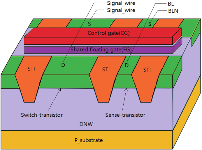
    Fig. 1. (Color online) Structure of Flash switch unit.
    (Color online) N-channel Flash. (a) Program(FN). (b) Threshold voltage distribution and adjust.
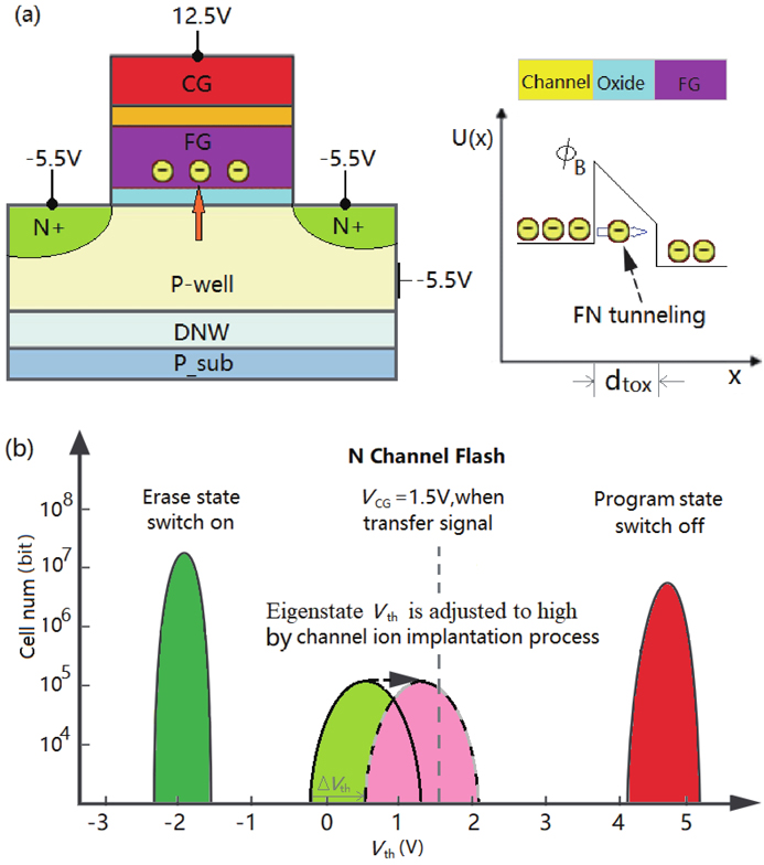
    Fig. 2. (Color online) N-channel Flash. (a) Program(FN). (b) Threshold voltage distribution and adjust.
    (Color online) P-channel Flash. (a) Program(BTBTIHE). (b) Threshold voltage distribution and adjust.
    Fig. 3. (Color online) P-channel Flash. (a) Program(BTBTIHE). (b) Threshold voltage distribution and adjust.
    (Color online) Signal selector MUX use P-channel Flash.
    Fig. 4. (Color online) Signal selector MUX use P-channel Flash.
    (Color online) Measured eigenstate threshold voltage of the Flash switch.
    Fig. 5. (Color online) Measured eigenstate threshold voltage of the Flash switch.
    (Color online) Energy band diagram of the Flash cell.
    Fig. 6. (Color online) Energy band diagram of the Flash cell.
    (Color online) Spectrum of ultraviolet light.
    Fig. 7. (Color online) Spectrum of ultraviolet light.
    (Color online) Ultraviolet light erasing.
    Fig. 8. (Color online) Ultraviolet light erasing.
    (Color online) Metal wiring of Flash-based FPGA.
    Fig. 9. (Color online) Metal wiring of Flash-based FPGA.
    (Color online) Relationship between threshold voltage drift and baking time.
    Fig. 10. (Color online) Relationship between threshold voltage drift and baking time.
    (Color online) Energy band diagram of floating gate structure under X-ray radiation ionization. (a) Programming state. (b) Erasing state.
    Fig. 11. (Color online) Energy band diagram of floating gate structure under X-ray radiation ionization. (a) Programming state. (b) Erasing state.
    (Color online) Two logic control schemes for the first power-on. (a) Control the Flash gate. (b) Control the GND of core logic.
    Fig. 12. (Color online) Two logic control schemes for the first power-on. (a) Control the Flash gate. (b) Control the GND of core logic.
    (Color online) Voltage control of Flash cell gate.
    Fig. 13. (Color online) Voltage control of Flash cell gate.
    (Color online) GND to L_GND channel.
    Fig. 14. (Color online) GND to L_GND channel.
    (Color online) Control logic of L_GND channel switch.
    Fig. 15. (Color online) Control logic of L_GND channel switch.
    (Color online) Competition between voltage and current during power-on.
    Fig. 16. (Color online) Competition between voltage and current during power-on.
    Flash cell PCM.
    Fig. 17. Flash cell PCM.
    (Color online) A 3.5 million Flash-based FPGA.
    Fig. 18. (Color online) A 3.5 million Flash-based FPGA.
    (Color online) UVC irradiation test. (a) Flash cell PCM. (b) Flash-based FPGA.
    Fig. 19. (Color online) UVC irradiation test. (a) Flash cell PCM. (b) Flash-based FPGA.
    (Color online) X-ray irradiation test. (a) Flash cell PCM. (b) Flash-based FPGA.
    Fig. 20. (Color online) X-ray irradiation test. (a) Flash cell PCM. (b) Flash-based FPGA.
    (Color online) High temperature baking test. (a) Flash cell PCM. (b) Flash-based FPGA.
    Fig. 21. (Color online) High temperature baking test. (a) Flash cell PCM. (b) Flash-based FPGA.
    (Color online) Power-on waveform. (a) Circuit without path control of power supply. (b) Circuit with path control of power supply.
    Fig. 22. (Color online) Power-on waveform. (a) Circuit without path control of power supply. (b) Circuit with path control of power supply.
    (Color online) Power-on current of the circuit with path control of power supply at –55, 25 and 125 °C.
    Fig. 23. (Color online) Power-on current of the circuit with path control of power supply at –55, 25 and 125 °C.
    MethodLeakage current ofFlash cellPower-on current of FPGATime con-sumptionCost
    UVC irradiationGoodPoorMediumGood
    High temperature bakingPoorPoorPoorGood
    X-ray irradiationGoodPoorMediumMedium
    Circuit logic controlGoodGoodMedium
    Table 1. Comparison of four methods.
    Yueer Shan, Zhengzhou Cao, Guozhu Liu. Research on eigenstate current control technology of Flash-based FPGA[J]. Journal of Semiconductors, 2022, 43(12): 122401
    Download Citation