• Photonics Research
  • Vol. 10, Issue 5, 1194 (2022)
Jinchao Tong1、4, Heng Luo2, Fei Suo1, Tianning Zhang1, Dawei Zhang3, and Dao Hua Zhang1、*
Author Affiliations
  • 1School of Electrical and Electronic Engineering, Nanyang Technological University, Singapore 639798, Singapore
  • 2School of Physics and Electronics, Central South University, Changsha 410083, China
  • 3Ministry of Education and Shanghai Key Laboratory of Modern Optical System, University of Shanghai for Science and Technology, Shanghai 200093, China
  • 4e-mail: jctong64@163.com
  • show less
    DOI: 10.1364/PRJ.444354 Cite this Article Set citation alerts
    Jinchao Tong, Heng Luo, Fei Suo, Tianning Zhang, Dawei Zhang, Dao Hua Zhang. Epitaxial indium antimonide for multiband photodetection from IR to millimeter/terahertz wave[J]. Photonics Research, 2022, 10(5): 1194 Copy Citation Text show less
    Design of the epitaxial IR-millimeter/THz wave multiband photodetector. (a) Structure of the epitaxial InSb on GaAs. (b) Relative permittivity of InSb in the millimeter/terahertz wave range followed by a Drude model. (c) Schematic of the multiband detector. A planar log-period antenna is adopted to couple the millimeter/terahertz wave. IR wave impinges on the surface of the InSb mesa. Inset is the microscope image of the detector and the scale bar represents 50 μm. (d) Typical field distribution by the couple of the antenna calculated by Ansys HFSS software. In the Ansys HFSS antenna simulation, the electromagnetic wave is fed at the gap with an impedance of 50 Ω. (e) E plane and H plane of the antenna. (f) Typical distribution of |E|2 near the central Au-InSb-Au structure calculated by COMSOL Multiphysics software. PML boundary condition is adopted in the simulation. The incident light is polarized along the direction of the y axis to meet the experiments. Distribution of |E|2 along (g) the cut-line I and (h) the cut-line II in (f).
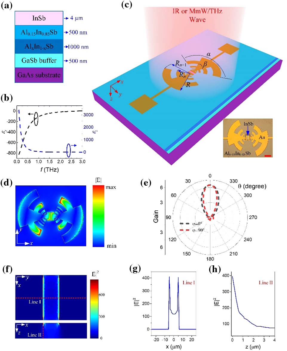
    Fig. 1. Design of the epitaxial IR-millimeter/THz wave multiband photodetector. (a) Structure of the epitaxial InSb on GaAs. (b) Relative permittivity of InSb in the millimeter/terahertz wave range followed by a Drude model. (c) Schematic of the multiband detector. A planar log-period antenna is adopted to couple the millimeter/terahertz wave. IR wave impinges on the surface of the InSb mesa. Inset is the microscope image of the detector and the scale bar represents 50 μm. (d) Typical field distribution by the couple of the antenna calculated by Ansys HFSS software. In the Ansys HFSS antenna simulation, the electromagnetic wave is fed at the gap with an impedance of 50 Ω. (e) E plane and H plane of the antenna. (f) Typical distribution of |E|2 near the central Au-InSb-Au structure calculated by COMSOL Multiphysics software. PML boundary condition is adopted in the simulation. The incident light is polarized along the direction of the y axis to meet the experiments. Distribution of |E|2 along (g) the cut-line I and (h) the cut-line II in (f).
    Dark current and noise of the detector. (a) Current–voltage (I–V) characteristic curves of the detector at temperatures from 293 to 170 K. (b) Calculated voltage noise of the detector with respect to bias at different temperatures.
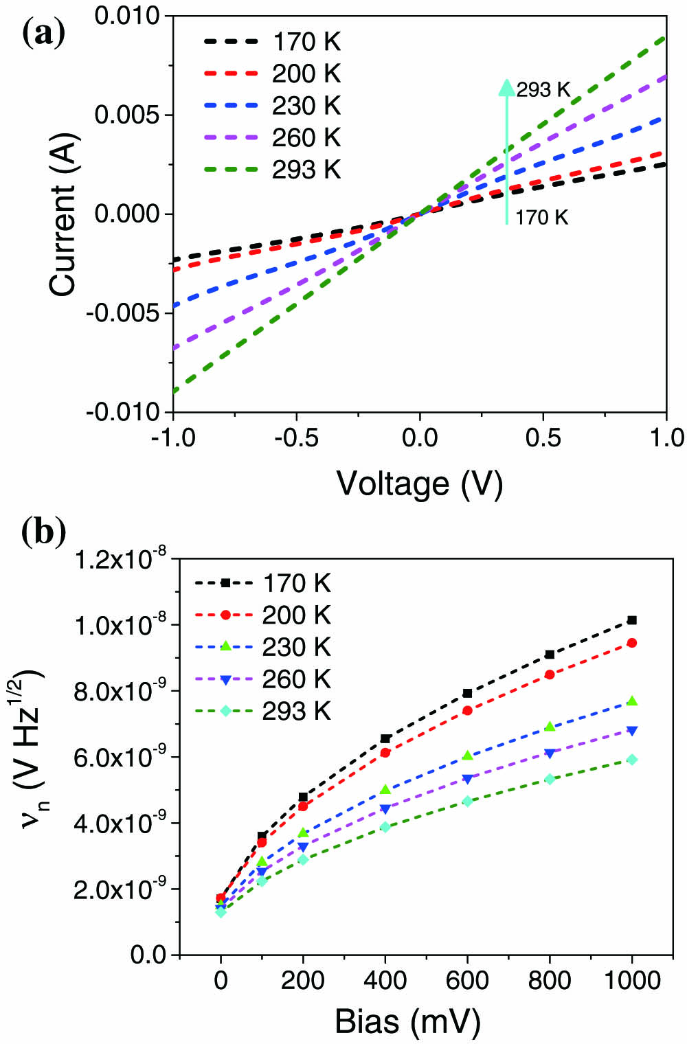
    Fig. 2. Dark current and noise of the detector. (a) Current–voltage (IV) characteristic curves of the detector at temperatures from 293 to 170 K. (b) Calculated voltage noise of the detector with respect to bias at different temperatures.
    Characterization of the detector for IR wave detection. (a) Relative spectral response of the detector at different temperatures. (b) Blackbody responsivity of the detector with respect to bias at different temperatures. (c) Blackbody responsivity of the detector at different temperatures under an applied voltage bias of 1000 mV. (d) Blackbody detectivity of the detector with respect to bias at different temperatures. (e) Blackbody detectivity of the detector at different temperatures under an applied voltage bias of 1000 mV.
    Fig. 3. Characterization of the detector for IR wave detection. (a) Relative spectral response of the detector at different temperatures. (b) Blackbody responsivity of the detector with respect to bias at different temperatures. (c) Blackbody responsivity of the detector at different temperatures under an applied voltage bias of 1000 mV. (d) Blackbody detectivity of the detector with respect to bias at different temperatures. (e) Blackbody detectivity of the detector at different temperatures under an applied voltage bias of 1000 mV.
    Response speed of the detector for IR. (a) Typical response waveform of the detector under illumination of a 2.94 μm laser with rise time of 20 ns. (b) Normalized amplitude frequency response of the detector.
    Fig. 4. Response speed of the detector for IR. (a) Typical response waveform of the detector under illumination of a 2.94 μm laser with rise time of 20 ns. (b) Normalized amplitude frequency response of the detector.
    Characterization of the detector at 0.270 THz. (a) Responsivity and NEP of the detector with respect to bias at 0.270 THz. (b) Responsivity and NEP of the detector with respect to temperature under an applied voltage bias of 1000 mV.
    Fig. 5. Characterization of the detector at 0.270 THz. (a) Responsivity and NEP of the detector with respect to bias at 0.270 THz. (b) Responsivity and NEP of the detector with respect to temperature under an applied voltage bias of 1000 mV.
    Multispectral response of the detector for a millimeter/terahertz wave under an applied bias of 1000 mV. (a) Responsivity. (b) NEP. Performances of three commercial VDI modules are also plotted for comparison.
    Fig. 6. Multispectral response of the detector for a millimeter/terahertz wave under an applied bias of 1000 mV. (a) Responsivity. (b) NEP. Performances of three commercial VDI modules are also plotted for comparison.
    Response speed of the detector for a millimeter/terahertz wave. (a) Normalized amplitude frequency response of the detector at 0.270 THz at different temperatures. (b) The f−3dB value and corresponding rise time of the detector derived from (a).
    Fig. 7. Response speed of the detector for a millimeter/terahertz wave. (a) Normalized amplitude frequency response of the detector at 0.270 THz at different temperatures. (b) The f3dB value and corresponding rise time of the detector derived from (a).
    TechnologyNEP (WHz1/2)Frequency (THz)Speed (s)
    Golay cells [9]10101090.02–30(2.55)×102
    Pyroelectric [45]109<30101
    Schottky diodes [36]10120.075–0.110 (WR10); 0.140–0.220 (WR5.1); 0.220–0.330 (WR3.4)<109
    Bolometers (HgCdTe, SiGe, Ti, NbN, VOx, Nb, Al/Nb) [1]1011109<3106103
    Si FET or Si CMOS [46,47]10111010<0.7
    CMOS-based (SiGe, GaAs/AlGaAs, InGaAs, InGaP/InGaAs/GaAs, GaN/AlGaN) [1]1011109<3
    Photoconductive antenna [3,48]0.1–1.5 (depending on antenna)<109
    InAs/AlSb/AlGaSb [49]1.8×10130.094109
    AlGaN/GaN [6]5.8×10130.14
    InAlAs/InGaAs/InP [50]4.8×10130.2–0.292
    InSb/AlInSb/GaSb/GaAs (this work)1.0×10130.032–0.3301.5×105
    Table 1. Comparison of Uncooled Performance to State-of-the-Art Technologies for Millimeter/THz Wave
    Jinchao Tong, Heng Luo, Fei Suo, Tianning Zhang, Dawei Zhang, Dao Hua Zhang. Epitaxial indium antimonide for multiband photodetection from IR to millimeter/terahertz wave[J]. Photonics Research, 2022, 10(5): 1194
    Download Citation