
Jinchao Tong, Heng Luo, Fei Suo, Tianning Zhang, Dawei Zhang, Dao Hua Zhang, "Epitaxial indium antimonide for multiband photodetection from IR to millimeter/terahertz wave," Photonics Res. 10, 1194 (2022)
- Photonics Research
- Vol. 10, Issue 5, 1194 (2022)
Abstract
1. INTRODUCTION
Photodetection converts light into an electrical signal, which can help to acquire spectral information radiated or scattered from objectives. Conventional solid-state photodetectors are usually only able to deal with spectral information within a single electromagnetic waveband due to the existence of a characteristic energy gap that quantum photons must overcome. A multiband detection capability is highly desirable because it can conduct multispectral information discrimination, identification, and processing. The current development of multiband epitaxial solid-state detectors mainly focuses on detector technologies such as HgCdTe, quantum well IR photodetectors (QWIPs), antimonide-based type-II superlattices, and quantum dot IR photodetectors (QDIPs) [1]. However, these technologies only target short-wavelength IR (SWIR) to middle-wavelength IR (MWIR) and long-wavelength IR (LWIR). It is still quite hard to use them for millimeter/terahertz wave detection [2–6] due to the extremely low quantum energy of millimeter/terahertz photons, which, on the one hand, limits the carriers’ transition in conventional optoelectrical semiconductors; on the other hand, it is vulnerable to strong background thermal disturbance.
Thermal-detection is a strategy to realize multispectral band detection. For example,
Indium antimonide (InSb) is a III-V group semiconductor that has a bandgap of
Sign up for Photonics Research TOC. Get the latest issue of Photonics Research delivered right to you!Sign up now
One of the outstanding capabilities of plasmonic InSb under the radiation of a millimeter/terahertz wave is that the decay of SPPs can boost the generation of nonequilibrium electrons [17–22]. As a result, a new strategy to realize the detection of long wavelength millimeter/terahertz photons has been proposed [23,24]. In an antenna-coupled ohmic metal–semiconductor–metal configuration, SPPs will be excited in the plasmonic semiconductor under the illumination of a millimeter/terahertz wave. The decay of SPPs then induces nonequilibrium electrons that can form a photocurrent/photovoltage under an external bias. This strategy based on SPPs in semiconductors opens a new avenue to develop sensitive millimeter/terahertz wave detectors.
Here, we report an epitaxially grown InSb on a GaAs substrate for multiband photodetection from the IR to a millimeter/terahertz wave. InSb is a III-V group semiconductor with a bandgap of
2. EXPERIMENTAL METHODS
A. Device Design and Simulation
The epitaxial structure was grown on a GaAs substrate by molecular beam epitaxy (MBE). As shown in Fig. 1(a), it contains a GaSb buffer layer (500 nm), an
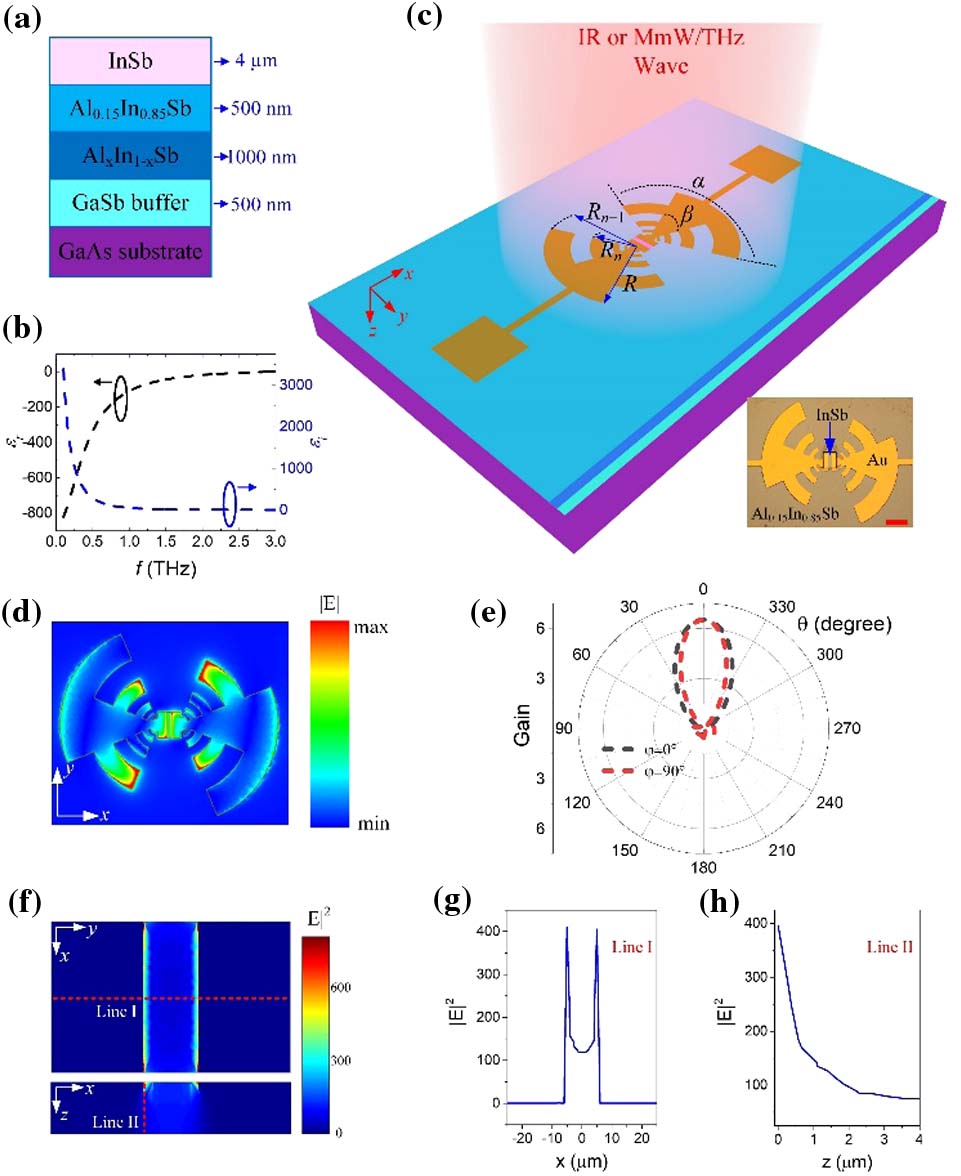
Figure 1.Design of the epitaxial IR-millimeter/THz wave multiband photodetector. (a) Structure of the epitaxial InSb on GaAs. (b) Relative permittivity of InSb in the millimeter/terahertz wave range followed by a Drude model. (c) Schematic of the multiband detector. A planar log-period antenna is adopted to couple the millimeter/terahertz wave. IR wave impinges on the surface of the InSb mesa. Inset is the microscope image of the detector and the scale bar represents 50 μm. (d) Typical field distribution by the couple of the antenna calculated by Ansys HFSS software. In the Ansys HFSS antenna simulation, the electromagnetic wave is fed at the gap with an impedance of 50 Ω. (e)
The design and microscope image of the multiband detector are shown in Fig. 1(c). A metallic planar log-period antenna [25,26] is used to couple a millimeter/terahertz wave to the central active InSb mesa. In the design of this antenna, the geometric ratio is
B. Device Fabrication and Characterization
In detector fabrication, the mesa was formed by a chemical solution (
A commercial Virginia Diodes tunable synthesizer (0.008–0.020 THz), a WR28SGX (signal generator extension module 0.026–0.040 THz), a WR10SGX-M (mini signal generator extension module 0.075–0.110 THz), a
3. RESULTS
A. Current–Voltage Characterization
Figure 2(a) plots the measured current–voltage (I–V) characteristic curves of the detector at temperatures from 293 to 170 K. They show good linear and symmetric characters, demonstrating good Au/Ti-InSb ohmic contacts in the detector and, therefore, excluding the potential disturbance of a Schottky barrier in the photodetection. The resistance of the detector is found to be increased from
![]()
Figure 2.Dark current and noise of the detector. (a) Current–voltage (
B. Photoresponse for IR Band
Figure 3(a) shows the relative spectral responses of the detector for an IR wave at different temperatures. At 293 K, it has a long wavelength 100% cutoff at 6.85 μm, which shows a blueshift to 6.44 μm while decreasing the temperature to 170 K. The shift of the cutoff wavelength follows that of the bandgap of InSb. Figure 3(b) shows that blackbody responsivity increases with an increase in the bias at different temperatures. As for the IR wave, the detector here is actually a photoconductor and its responsivity can be expressed as [1]
![]()
Figure 3.Characterization of the detector for IR wave detection. (a) Relative spectral response of the detector at different temperatures. (b) Blackbody responsivity of the detector with respect to bias at different temperatures. (c) Blackbody responsivity of the detector at different temperatures under an applied voltage bias of 1000 mV. (d) Blackbody detectivity of the detector with respect to bias at different temperatures. (e) Blackbody detectivity of the detector at different temperatures under an applied voltage bias of 1000 mV.
To evaluate the response speed of the detector for an IR wave, a 2.94 μm laser source with maximum modulation frequency up to 1 MHz is used to pump the detector. The rise time of the square wave source is 20 ns. The output power of the source is found to be stable to ensure reliable measurements. Figure 4(a) shows the typical response waveform of the detector at room temperature. A rise time as fast as 800 ns (or
![]()
Figure 4.Response speed of the detector for IR. (a) Typical response waveform of the detector under illumination of a 2.94 μm laser with rise time of 20 ns. (b) Normalized amplitude frequency response of the detector.
C. Photoresponse for Millimeter/Terahertz Bands
The performance of our detector was also characterized for a millimeter/terahertz wave. Figure 5(a) shows the measured
![]()
Figure 5.Characterization of the detector at 0.270 THz. (a) Responsivity and NEP of the detector with respect to bias at 0.270 THz. (b) Responsivity and NEP of the detector with respect to temperature under an applied voltage bias of 1000 mV.
The spectral response was characterized in Fig. 6 for a broad millimeter/terahertz wave range from 0.032 to 0.330 THz (or from
![]()
Figure 6.Multispectral response of the detector for a millimeter/terahertz wave under an applied bias of 1000 mV. (a) Responsivity. (b) NEP. Performances of three commercial VDI modules are also plotted for comparison.
![]()
Figure 7.Response speed of the detector for a millimeter/terahertz wave. (a) Normalized amplitude frequency response of the detector at 0.270 THz at different temperatures. (b) The
4. CONCLUSION
In conclusion, we present an epitaxially grown InSb on GaAs for multiband photodetection from IR to millimeter/terahertz wave. The detection for an IR wave is based on an interband transition in InSb, and a blackbody detectivity of
Acknowledgment
Acknowledgment. J. Tong acknowledges support from Nanyang Technological University Presidential Postdoctoral Fellowship and help from Dr. Bingxuan Li, Dr. Gang Yih Chong, and Ms. Ling Ngo. The device fabrication was carried out at the Nanyang NanoFabrication Centre (N2FC).
References
[1] A. Rogalski. Infrared and Terahertz Detectors(2019).
[2] R. A. Lewis. A review of terahertz detectors. J. Phys. D, 52, 433001(2019).
[3] K. Peng, P. Parkinson, L. Fu, Q. Gao, N. Jiang, Y.-N. Guo, F. Wang, H. J. Joyce, J. L. Boland, H. H. Tan, C. Jagadish, M. B. Johnston. Single nanowire photoconductive terahertz detectors. Nano Lett., 15, 206-210(2015).
[4] K. Peng, D. Jevtics, F. Zhang, S. Sterzl, D. A. Damry, M. U. Rothmann, B. Guilhabert, M. J. Strain, H. H. Tan, L. M. Herz, L. Fu, M. D. Dawson, A. Hurtado, C. Jagadish, M. B. Johnston. Three-dimensional cross-nanowire networks recover full terahertz state. Science, 368, 510-513(2020).
[5] N. Wang, S. Cakmakyapan, Y.-J. Lin, H. Javadi, M. Jarrahi. Room-temperature heterodyne terahertz detection with quantum-level sensitivity. Nat. Astron., 3, 977-982(2019).
[6] H. W. Hou, Z. Liu, J. H. Teng, T. Palacios, S. J. Chua. High temperature terahertz detectors realized by a GaN high electron mobility transistor. Sci. Rep., 7, 46664(2017).
[7] P. L. Richards. Bolometers for IR and millimeter waves. J. Appl. Phys., 76, 1-24(1994).
[8] F. Sizov. Terahertz radiation detectors: the state-of-the-art. Semicond. Sci. Technol., 33, 123001(2018).
[10] A. Rogalski, M. Kopytko, P. Martyniuk. Two-dimensional infrared and terahertz detectors: outlook and status. Appl. Phys. Rev., 6, 021316(2019).
[11] Q. Qiu, Z. Huang. Photodetectors of 2D materials from ultraviolet to terahertz waves. Adv. Mater., 33, 2008126(2021).
[12] V. Giannini, A. Berrier, S. A. Maier, J. A. Sánchez-Gil, J. G. Rivas. Scattering efficiency and near field enhancement of active semiconductor plasmonic antennas at terahertz frequencies. Opt. Express, 18, 2797-2807(2010).
[13] L. Deng, J. Teng, H. Liu, Q. Y. Wu, J. Tang, X. Zhang, S. A. Maier, K. P. Lim, C. Y. Ngo, S. F. Yoon, S. J. Chua. Direct optical tuning of the terahertz plasmonic response of InSb subwavelength gratings. Adv. Opt. Mater., 1, 128-132(2013).
[14] S. M. Hanham, A. I. Fernández-Domínguez, J. H. Teng, S. S. Ang, K. P. Lim, S. F. Yoon, C. Y. Ngo, N. Klein, J. B. Pendry, S. A. Maier. Broadband terahertz plasmonic response of touching InSb disks. Adv. Mater., 24, OP226-OP230(2012).
[15] R. Parthasarathy, A. Bykhovski, B. Gelmont, T. Globus, N. Swami, D. Woolard. Enhanced coupling of subterahertz radiation with semiconductor periodic slot arrays. Phys. Rev. Lett., 98, 153906(2007).
[16] G. Jaime, C. Janke, P. H. Bolivar, H. Kurz. Transmission of THz radiation through InSb gratings of subwavelength apertures. Opt. Express, 13, 847-859(2005).
[17] R. Sundararaman, P. Narang, A. S. Jermyn, W. A. Goddard, H. A. Atwater. Theoretical predictions for hot-carrier generation from surface plasmon decay. Nat. Commun., 5, 5788(2014).
[18] C. Clavero. Plasmon-induced hot-electron generation at nanoparticle/metal-oxide interfaces for photovoltaic and photocatalytic devices. Nat. Photonics, 8, 95-103(2014).
[19] J. Lehmann, M. Merschdorf, W. Pfeiffer, A. Thon, S. Voll, G. Gerber. Surface plasmon dynamics in silver nanoparticles studied by femtosecond time-resolved photoemission. Phys. Rev. Lett., 85, 2921-2924(2000).
[20] K. Wu, J. Chen, J. R. McBride, T. Lian. Efficient hot-electron transfer by a plasmon-induced interfacial charge-transfer transition. Science, 349, 632-635(2015).
[21] M. W. Knight, H. Sobhani, P. Nordlander, N. J. Halas. Photodetection with active optical antennas. Science, 332, 702-704(2011).
[22] A. Giugni, B. Torre, A. Toma, M. Francardi, M. Malerba, A. Alabastri, R. Proietti Zaccaria, M. I. Stockman, E. Di Fabrizio. Hot-electron nanoscopy using adiabatic compression of surface plasmons. Nat. Nanotechnol., 8, 845-852(2013).
[23] J. Tong, W. Zhou, Y. Qu, Z. Xu, Z. Huang, D. H. Zhang. Surface plasmon induced direct detection of long wavelength photons. Nat. Commun., 8, 1660(2017).
[24] J. Tong, F. Suo, T. Zhang, Z. Huang, J. Chu, D. H. Zhang. Plasmonic semiconductor nanogroove array enhanced broad spectral band millimetre and terahertz wave detection. Light Sci. Appl., 10, 58(2021).
[25] C. Balanis. Antenna Theory: Analysis and Design(2016).
[26] R. DuHamel, F. Ore. Logarithmically periodic antenna designs. IRE International Convention Record, 6, 139-151(2005).
[27] L. Vicarelli, M. S. Vitiello, D. Coquillat, A. Lombardo, A. C. Ferrari, W. Knap, M. Polini, V. Pellegrini, A. Tredicucci. Graphene field-effect transistors as room-temperature terahertz detectors. Nat. Mater., 11, 865-871(2012).
[28] L. Viti, J. Hu, D. Coquillat, W. Knap, A. Tredicucci, A. Politano, M. S. Vitiello. Black phosphorus terahertz photodetectors. Adv. Mater., 27, 5567-5572(2015).
[29] Y. Li, Y. Zhang, T. Li, M. Li, Z. Chen, Q. Li, H. Zhao, Q. Sheng, W. Shi, J. Yao. Ultrabroadband, ultraviolet to terahertz, and high sensitivity CH3NH3PbI3 perovskite photodetectors. Nano Lett., 20, 5646-5654(2020).
[30] Y. Chen, Y. Wang, Z. Wang, Y. Gu, Y. Ye, X. Chai, J. Ye, Y. Chen, R. Xie, Y. Zhou, Z. Hu, Q. Li, L. Zhang, F. Wang, P. Wang, J. Miao, J. Wang, X. Chen, W. Lu, P. Zhou, W. Hu. Unipolar barrier photodetectors based on van der Waals heterostructures. Nat. Electron., 4, 357-363(2021).
[31] Y. Fang, A. Armin, P. Meredith, J. Huang. Accurate characterization of next-generation thin-film photodetectors. Nat. Photonics, 13, 1-4(2019).
[32] . InSb photoconductive detectors.
[33] . InAsSb photovoltaic detectors.
[35] J. Yan, M. H. Kim, J. A. Elle, A. B. Sushkov, G. S. Jenkins, H. M. Milchberg, M. S. Fuhrer, H. D. Drew. Dual-gated bilayer graphene hot-electron bolometer. Nat. Nanotechnol., 7, 472-478(2012).
[36] Virginia Diodes,. Detectors.
[37] D. Pozar. Considerations for millimeter wave printed antennas. IEEE Trans. Antennas Propag., 31, 740-747(1983).
[38] A. Dhiflaoui, A. Yahyaoui, J. Yousaf, T. Aguili, B. Hakim, H. Rmili, R. Mittra. Full wave numerical analysis of wideband and high directive log spiral THz photoconductive antenna. Int. J. Numer. Model. Electron. Netw. Devices Fields, 33, e2761(2020).
[39] M. Sakhno, J. Gumenjuk-Sichevska, F. Sizov. Modeling of the substrate influence on multielement THz detector operation. J. Infrared Millim. Terahertz Waves, 35, 703-719(2014).
[40] T. K. Nguyen, T. A. Ho, H. Han, I. Park. Numerical study of self-complementary antenna characteristics on substrate lenses at terahertz frequency. J. Infrared Millim. Terahertz Waves, 33, 1123-1137(2012).
[41] E. N. Grossman, A. J. Miller. Active millimeter-wave imaging for concealed weapons detection. Proc. SPIE, 5077, 62(2003).
[42] X.-C. Tu, L. Kang, X.-H. Liu, Q.-K. Mao, C. Wan, J. Chen, B.-B. Jin, Z.-M. Ji, W.-W. Xu, P.-H. Wu. Nb5N6 microbolometer arrays for terahertz detection. Chin. Phys. B, 22, 040701(2013).
[43] I. Kašalynas, R. Venckevičius, L. Minkevičius, A. Sešek, F. Wahaia, V. Tamošiūnas, B. Voisiat, D. Seliuta, G. Valušis, A. Švigelj, J. Trontelj. Spectroscopic terahertz imaging at room temperature employing microbolometer terahertz sensors and its application to the study of carcinoma tissues. Sensors, 16, 432(2016).
[44] D. Rutledge, S. Schwarz. Planar multimode detector arrays for infrared and millimeter-wave applications. IEEE J. Quantum Electron., 17, 407-414(1981).
[45] QMC Instruments. Terahertz pyroelectric detectors.
[46] R. Tauk, F. Teppe, S. Boubanga, D. Coquillat, W. Knap, Y. M. Meziani, C. Gallon, F. Boeuf, T. Skotnicki, C. Fenouillet-Beranger, D. K. Maude, S. Rumyantsev, M. S. Shur. Plasma wave detection of terahertz radiation by silicon field effects transistors: responsivity and noise equivalent power. Appl. Phys. Lett., 89, 253511(2006).
[47] U. R. Pfeiffer, E. Ojefors. Terahertz imaging with CMOS/BiCMOS process technologies. Proceedings of European Solid State Circuits Conference (ESSCIRC), 52-60(2010).
[48] E. Castro-Camus, J. Lloyd-Hughes, M. B. Johnston, M. D. Fraser, H. H. Tan, C. Jagadish. Polarization-sensitive terahertz detection by multicontact photoconductive receivers. Appl. Phys. Lett., 86, 254102(2005).
[49] Z. Zhang, R. Rajavel, P. Deelman, P. Fay. Sub-micron area heterojunction backward diode millimeter-wave detectors with 0.18 pW/Hz1/2 noise equivalent power. IEEE Microw. Wirel. Components Lett., 21, 267-269(2011).
[50] Y. Kurita, G. Ducournau, D. Coquillat, A. Satou, K. Kobayashi, S. B. Tombet, Y. M. Meziani, V. V. Popov, W. Knap, T. Suemitsu, T. Otsuji. Ultrahigh sensitive sub-terahertz detection by InP-based asymmetric dual-grating-gate high-electron-mobility transistors and their broadband characteristics. Appl. Phys. Lett., 104, 251114(2014).


Set citation alerts for the article
Please enter your email address

© Copyright 2018-2021 | Chinese Laser Press. All Rights Reserved 沪ICP备15018463号-20